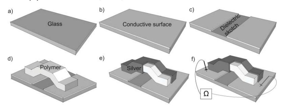
There has been a lot of interest recently in the design and fabrication of three-dimensional (3D) metallic micro/nanostructures for applications in micro-electro mechanical systems (MEMS) [1], plasmonics [2], biosensors [3], and optical metamaterials [4]. However, the fabrication of complex, high resolution, fully 3D metallic structures is still a challenging task, since traditional lithographic techniques, involving the layer-by-layer structuring of metallic structures, can only allow the deposition of a few layers or the creation of high-aspect ratio two-dimensional (2D) structures.
As an alternative technology for fabrication of 3D metallic micro/nanostructures ultrafast lasers can be used. There are three main methods: multiphoton reduction of metal ions [5], direct laser writing into a positive-tone photoresist followed by electrochemical deposition of metal [6], and direct laser writing of negative photoresists and subsequent metallization of the 3D nanostructures using electroless plating [7].
The third method has attracted the most attention up-to date and has been chosen for this work. It allows to create dielectric nanostructures with sub-100 nm resolution and metallize them without external source of electric current. It is characterised by the selective reduction of metal ions only at the surface of a catalytic substrate immersed into an aqueous solution of metal ions.
In this report, we present study of possibility to connect two conductive surfaces with metallized polymeric link and defining it's properties. Conductive surfaces were separated by laser ablated dielectric skotch. Zirconium containing organic-inorganic photosensitive material doped with amine metal-binding moieties was used for fabrication of the structure [7]. Then it was chemically metallized with silver and measurements of resistance were made. It was shown that metallized polymeric links are conductive, however, dielectric skotches also were covered with some silver.