
Global demand for energy is increasing. The direct conversion of sunlight into electrical energy can be the most potential alternative to fossil fuels and a preferred method for clean and safe energy production in the future [1, 2]. Thin film solar cell technologies have raised the expectation that photovoltaics will be able to compete with traditional energy production methods due to expected lower processing costs [2]. Among various thin film absorbers the main interest are amorphous Si, CdTe and CuInSe2 and its alloys with Ga and/or S [1]. CIGS thin film solar cells have a high optical absorption coefficient and a tunable band gap [2].
CIGS solar cells have to be divided into smaller cells interconnected in series to avoid high currents and heat releasing. Three scribing processes are needed to form interconnect: P1 separates the molybdenum back contact, P2 connects the front contact with the back contact of the neighboring cell and P3 is necessary for the electrical separation of the conductive window [3].
In our experiments we focused on P3 scribing process to expose the molybdenum back contact. Three thin-film structures with different front contacts were processed: ITO/ZnO/CdS/CIGS/Mo/PI, ZnO/CdS/CIGS/Mo/PI, ZnO:Al/ZnO/CdS/CIGS/Mo/PI. The best scribing regimes with the lowest damage to the molybdenum back contact were found and ablation thresholds with different number of laser pulses were measured for all samples.
CIGS thin film solar cells were scribed by changing laser scanning speed, repetition rate and pulse energy. Two experimental setups were used for the ablation and scribing processes. In the femtosecond system thin-film structures were scribed using PHAROS laser (300 fs, 100 kHz repetition rate, 1032 nm wavelength). The laser beam was focused with an objective lens with a focal length of 50 mm and XYZ stage was used for sample positioning. In the nanosecond system structures were processed with BALTIC HP laser (10 ns, 10 – 100 kHz repetition rate, 1064 nm wavelength), the laser beam was positioned with a galvanometer scanner and focused with an objective lens with a focal length of 80 mm. The scribing process was evaluated with an optical microscope and scanning electron microscope (SEM), chemical compounds were characterized with the x-ray energy dispersion spectrometer (EDS).
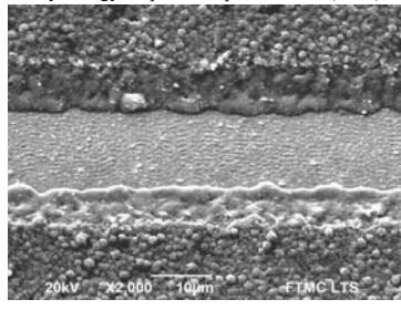
The best results with the femtosecond laser were achieved using $2.7 \mu J – 7 \mu J$ laser pulse energy and 60 – 160 mm/s laser scanning speed for ITO/ZnO/CdS/CIGS/Mo/PI sample, $1.1\mu J – 3.8 \mu J$ pulse energy and 40 – 200 mm/s scanning speed for ZnO/CdS/CIGS/Mo/PI sample and $1.5\mu J – 6.6\mu J$ pulse energy and 70 – 250 mm/s scanning speed for ZnO:Al/ZnO/CdS/CIGS/Mo/PI sample. We achieved less than 42 % melted edge compared to the whole width of the femtosecond laser scribe. While working with a nanosecond laser a clean scribe was not achieved and melted area was bigger compared to scribing with a femtosecond laser. Also melted edge area depended on the laser pulse energy and scanning speed. Results showed that scribing with lower laser pulse energy and slower scanning speed decreases melted area and provided sharper edges.