
Rapidly growing thin-film photovoltaic market is based on the CIGS technology - the most efficient technology for converting sunlight into electricity. On the other hand, the commercialized high-volume production of CIGS-based modules has some limitations due to the scarcity of indium and gallium and the environmental issues associated with Selenium [1]. To overcome these limitations, it has been proposed that CIGS can be replaced by Cu2ZnSn(S,Se)4 (CZTS) kesterite compound while keeping remaining structure elements the same [2]. This technology shows efficiencies up to 11.1% [3] for small scale devices.
The manufacturing costs and CZTS cell efficiency are critical factors for the wider applicability in terms of economical point of view. Efficiency of thin-film solar cells with a large active area might be maintained if small segments are interconnected in series in order to reduce photocurrent and resistance losses, and laser scribing is crucial for performance of the device. Previous investigations revealed some disadvantages of the direct laser ablation technique. Even working with femtosecond pulsed lasers it is almost impossible to avoid melted area formation at the edges of the laser scribed trench and degradation of electrical properties of the device.
For this we proposed laser induced material lift-off process for the front side scribing of the CZTS solar cells. Using proper laser wavelength, it is possible to control laser energy coupling in the complex film layer structure. High absorption at inner interface of the layers triggers localized rapid temperature rise which facilitates localized spallation of the films rather than evaporation. This material lift-off process enables to process thermally sensitive films as all the laser affected material is mechanically removed from the laser ablation area [4].
Ablation and scribing experiments were carried out with fundamental harmonics of the picosecond laser (Atlantic, 1064 nm, 10 ps, 50-500 kHz from EKSPLA).
Two types of multilayer structure of the CZTS solar cells were investigated: (i) complete structure consisting of TCO top-contact, Cu2ZnSn(S,Se)4 absorber layer, molybdenum back-contact and soda-lime-glass as a substrate and (ii) incomplete CZTS/Mo/SLG structure without top-contact.
Single pulse ablation and scribing experiments were performed on thin-film CZTS structure in order to find optimal conditions for the Mo back-contact exposure in both P2 and P3 processes. It was determined that at specific experimental conditions with sufficient laser beam focus off-set, constant and high repeatability lift-off craters could be formed (Fig. 1).
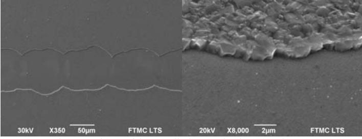
For trench scribing experiments, the P2 and P3 process speeds were limited by our scanning optics and were set to 1 m/s with laser repetition rates from 8 to 10 kHz depending on the process. Experimental results showed the potential of reaching high through output material lift-off based scribing processes for the CZTS thin-film solar cells with picosecond lasers.