
Diffractive optical elements showing high diffraction efficiencies have good optical quality for practical use [1]. Complex diffraction patterns require two-dimensional (2D) periodical structures that can be realised employing holographic lithography. There are two approaches how 2D structures can be realised employing holographic lithography: employing an interference pattern simultaneously generated by multiple beams or using multiple exposures of an interference optical field produced by two beams [2].
In this work we present 2D 0.4 – 1.1 µm period structures fabricated in positive tone photoresist layer employing multiple exposure holographic lithography technique. Different regular patterns were obtained changing the sample rotation angle between exposures and number of exposures. The resulting multiple exposure interference pattern intensities were calculated and the experimental angles were selected according to the targeted structures.
Fabricated structures were analyzed employing optical (see Fig. 1 a)) and scanning electron microscopy (SEM, see Fig. 1 b)). The diffraction efficiencies of diffraction maximums were measured (see Fig. 1 c)) and the spatial distribution of diffraction maximums was compared with Fast Fourier transformations (FFT) of SEM micrographs (see Fig. 1 d)).
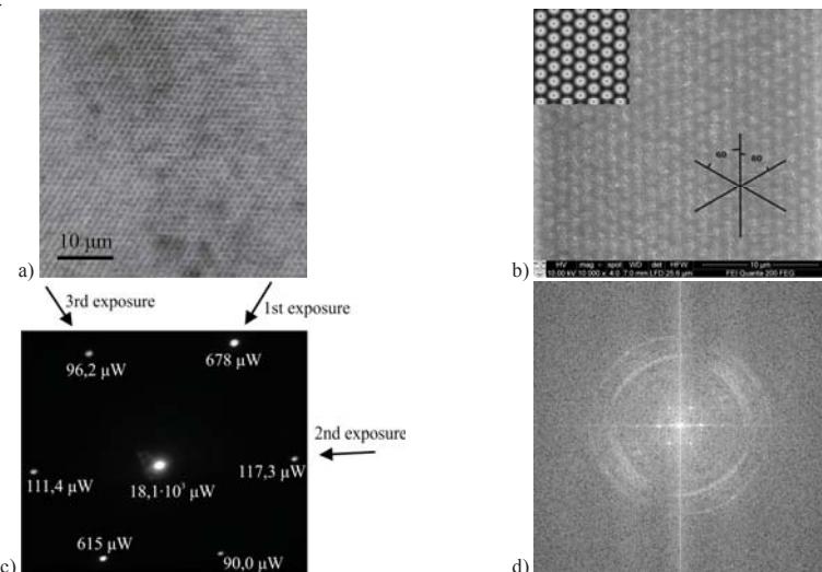
We have fabricated structures with period of 385 nm (angle of incidence: 33°) and 1.1 µm (angle of incidence: 10.5°). As seen in optical microscope images the fabricated periodical structures are even over large area. SEM micrographs show that calculated and fabricated structures are very similar. We have shown that multiple exposure holographic lithography is an effective method for fabrication of 2D periodic structures.