
The scribing of sapphire wafers is one of those areas where the correct usage of laser technologies might be the best tool for the optimization of the process [1, 2].
The development of light emitting diodes requires the most efficient technology of basis for the epitaxial GaN structuring. The unique physical, chemical and optical properties of a single crystal sapphire (Al2O3) such as structural fit between sapphire and GaN crystals, transparency at a wide range of wavelengths and a high thermal conductivity makes it an excellent material for the application [3].
In opposition to the widely used industrial methods: a blade dicing with a diamond disk or a laser ablation using nanosecond lasers at the range of ultraviolet wavelengths of irradiation, operating with a picosecond laser offers us a higher precision together with a new way to separate the pieces of the LED chips – the stealth dicing [4]. The greatness of this method is an internal processing that keeps us from any surface damage while still optimizing the process itself (Fig. 1).
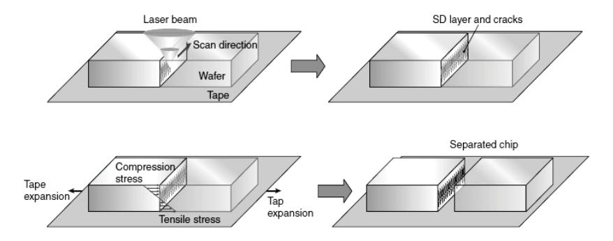
In this work, the intra-volume scribing of sapphire wafers with the picosecond laser pulses was investigated under various conditions of pulse energies and distances between laser pulses at 355 nm and 1064 nm wavelengths. The experiments led us to a significant improvement in the scribing of sapphire wafers. The stealth dicing was approved as the best method while it brought us to the foundation of an optical scribing system using both, 355 nm and 1064 nm, wavelengths at once.