Nanometer scale self-organized metal islands have a number of applications. They can be used in medicine to kill cancer cells selectively. Another field of application is optoelectronics [1-2]. At the interface between conductive particles and insulator or semiconductor the excitation of collective electrons, known as surface plasmons (SP), can be observed. The internal quantum efficiency of light emitting diode (LED) can be enhanced by coupling between dipoles in quantum wells (QW) and SPs. Experimentally the coupling can be observed by measuring transmittance spectra. At SP resonance frequency the intense light absorption is observed. The resonance frequency as well as wavelength of SPs can be tuned with change in the matter and diameter of metal nanoparticles. This allows obtaining an electromagnetic field enhancement in the wide range of energies.
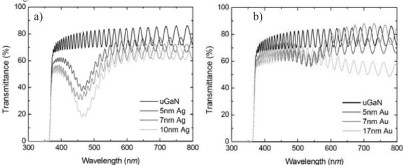
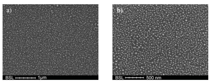
The nano-islands were prepared by depositing Au and Ag metal thin films of different thicknesses on undoped GaN/sapphire templates. GaN on sapphire was grown by metal organic chemical vapor deposition (MOCVD) technique. Afterwards samples were annealed at different temperatures by rapid thermal annealing (RTA). As the optical response of fabricated samples strongly depends on size and density of nano-islands, it is important to investigate the influence of various technological parameters: such as thickness of deposited metal layer, annealing temperature or time. In this work transmittance spectra were measured to determine the SP resonance. Fig. 1 shows transmittance spectra of samples with Ag and Au nano-islands on the surface. The absorption peaks were observed at 464 nm and 550 nm for Ag and Au samples respectively. Fig. 2 shows scanning electron microscopy (SEM) images of prepared samples. According to SEM image statistical analysis the size of nano-islands has an exponential distribution with the average mean diameter less than 50 nm.