
Nowadays new materials are in demand in the majority of human life activities. Various new material properties are needed for ecological safety and for material usability improving. One of the methods for new material production is modification of pre-surface layers by means of chemical, heat, radiation action and high energy flows. The use of compression plasma flows is of a great interest due to high energy density and short action time.
Compression plasma flows (CPF) are flows of compressed plasma generated by means of electrical discharge in the orifice gas atmosphere [1]. During treatment vacuum camera is filled by orifice gas (nitrogen, hydrogen, helium and etc.). Sample is placed against electrodes at the distance 8-20 cm. Plasma is formed by means of gas discharge while voltage supplying (1-5 kV). This plasma flows towards the sample and is compressed by its magnetic field. Therefore this plasma is compressed. The energy density near sample varies from 3 to 30 J/cm2 and action time is ~100 μs.
One of the CPF application is silicon based solar energy materials. It was discovered that compression plasma flows treatment of single-crystalline p-silicon (boron-doped) leads to the appearance of photovoltaic effect. The magnitude of free circuit voltages in this case is 150 – 300 mV. The advantages of this method in comparison with other is low vacuum requirements and short treatment time (~100 μs). The usual value of plasma modified silicon area is 1-2 cm2. This effect is observed when orifice gas is nitrogen. We suppose this effect to be connected with nitrogen penetration to the pre-surface layer and subsequent formation of n-layer because of nitrogen is donor for silicon.
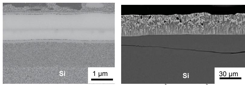
Another CPF application is the use for silicide layer formation. CPF action on silicon with pre-deposited metal coating leads to pre-surface silicide layer formation up to 30 μm depth. Modification process can be divided into two stages. On the first stage silicon and coating melt and intermixing takes place. It was found that intermixing mechanism depends upon plasma energy density Q [2]. If only diffusion takes place ($Q = 3-5 \text{ J/cm}^2$) structured interlayers of thickness 1 – 3 μm form (fig. 2a). If also convection takes place ($Q > 5 \text{ J/cm}^2$) the layer of thickness up to 30 μm forms (fig. 2b). The second stage is rapid cooling and solidification of the melted surface layer. The one leads to constitutional overcooling and subsequent formation of silicon dendrites with metal silicide (Ti5Si3, ZrSi2, CrSi2 and etc.) in interdendritic space. The tip radius of dendrites is typically 0.4 – 1 μm. The primary spacing is 0.5 – 1 μm.
Thereby CPF is a perspective tool for formation of silicon-based photovoltaic structures and silicide layers of thickness up to 30 μm. The formed silicides CrSi2 and ZrSi2 are perspective materials for electronic for interconnections, Ti5Si3 is of great interest as material for high temperature applications.