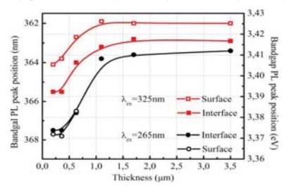
The development of undoped GaN epilayer at gradual stages of growth in the context of strain evolution was investigated by photoluminescence (PL) measurements. A series of samples of thickness from 200 nm to 3.5 μm corresponded to islets and continuous structure of epilayer, respectively. Surface and interface room temperature PL spectra measured under relative low cw excitation (1 W/cm2) evidenced quite well the evolution of blue (BL) and yellow (YL) photoluminescence spectra helping us to determine the structural transformations in due the course of growth.
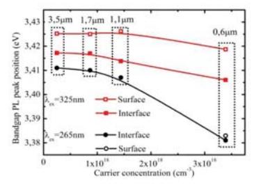
Shift of the bandgap PL to shorter wavelength on either side of the samples ($\lambda$=325 nm, 1 W/cm2 and $\lambda$=265 nm and 0.2 mW/cm2 excitation) with increasing epilayer thickness was observed (Fig. 1). Variant bandgap PL peak position correspondence to excitation depth demonstrates strain evolution in the epilayer volume. Plausible factors contributing to strain variation for different thick samples are: lattice thermal expansion coefficient mismatch between sapphire substrate and GaN, resulting in a residual compressive strain and coalescence of islets or presence of dopants initiating tensile strain [1-3]. Islets being relative small have perfect crystalline structure and are not affected by strain. Most threading dislocations at this stage would result only from island coalescence originating a tensile strain and redshifted bandgap PL. The observed blueshift, however, appears with sample thickness of 0.36 μm and saturates at 1.1 μm, what indicates rise and dominance of compressive stress in the structure of larger islet or even continuous structure overgrown (Fig. 1). For excitation light $\lambda$=325 nm and $\lambda$=265 nm the penetration depth is ~200 nm and ~100 nm, respectively: the shallower it is, the more relaxed compressive strain at the GaN/sapphire interface is, the longer wavelength is detected (Fig. 1), what correlates well with the conclusion about open site and stress reduction [3,4]. Relative higher energy bandgap PL detected from surface indicates in average higher compressive strain on this side, thus confirming about the more relaxed situation at the interface.
Considering reduction in compressive stress and bandgap narrowing effect, while increasing carrier concentration [5,6], the strain change in continuous structure overgrown samples (Fig. 2) in our case is explained unambiguously. At the start of coalescence islets due to relative high carrier concentration (up to $n \sim 3.5 \cdot 10^{18}$ cm-3) show red-shifted band-gap PL (Fig. 2): the formation of dislocation-type defects defines reduced compressive strain and more free carriers. In samples with continuous structure overgrown (from $d \sim 1.1 \, \mu m$) carrier concentration decreases and band-gap PL shifts to higher energies indicating the origination of compressive strain.