
Due to their low fabrication cost, pin-type hydrogenated amorphous silicon solar cells (a-Si:H SCs) are potential renewable solar energy sources. However, the device efficiency of a-Si:H SCs is still lower than that of poly-Si SCs. One method of improving device performances in a-Si:H SCs is to insert a transition metal oxide, such as tungsten oxide (WO3) between a textured fluorine-tin oxide (FTO) glass and a p-type Si layer as an adjusted p-type electrode. The WO3 layer increases carrier collection due to the band alignment between neighbouring layers in a-Si:H SCs and provides a large shunt resistance, which reduces carrier recombination at the interface [1].
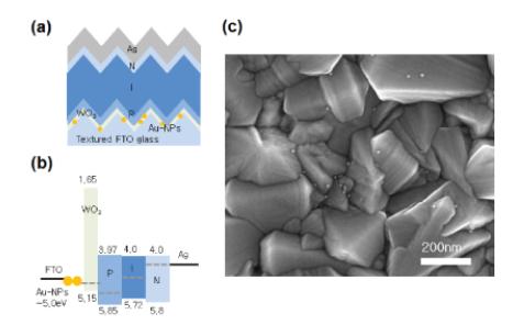
In our investigations a double layer of gold nano particles (Au-NPs) and amorphous tungsten oxide (a-WO3) was employed as a buffer layer on textured fluorine-tin oxide (FTO) glass in pin-type hydrogenated amorphous silicon solar cells (a-Si:H SCs), see Fig.1. Au-NPs of 10 nm size were spin coated and a-WO3 layer was thermally evaporated between Au-NPs on a FTO glass and hydrogenated amorphous p-type Si layer. a-Si:H SCs with a double buffer layer showed higher efficiency of 7% improvement, 8.059% from a value of 7.530%, and increased current density of 8.3% improvement, 14.212 mA/cm2 from a value of 13.120 mA/cm2, originating from the enhancement of electrical interface contact and bandgap alignment, as well as the slight absorption and surface plasmon resonance effect due to Au-NPs on textured FTO glass.
I-V characteristics and temperature dependencies of electrical dark and photo-conductivity of each structure were measured in the temperature range from 340 K down to 100K. Schottky barrier model was used to evaluate physical properties and characteristic parameters.
Carrier mobility measurements were performed by the CELIV (Charge Extraction by Linearly Increasing Voltage) method [2]. The voltage which is proportional to the current flowing through the sample was measured on the load resistor by oscilloscope. Another channel of the oscilloscope was used to measure the output signal of the generator. Carrier mobility was calculated from current kinetics according to the following expression:
$$\mu = \frac{d^2}{At^2_{\text{max}}(1 + 0.36\frac{\Delta i}{i(0)})} \tag{1}$$