
Type-I mid-infrared laser diodes based on GaSb have long been a promising material and technology platform for room-temperature laser diodes for the 2-4 μm wavelength range. However, long-wavelength laser diodes required complex materials such as quaternary GaInAsSb or AlGaAsSb and even quinternary AlGaInAsSb, which have been reported to be very demanding in terms of epitaxial growth and fabrication technology, in addition to thermal instability, known as the "blue shift" effect and the miscibility gap [1]. In our work, we demonstrate that AlxGayIn1-x-yAszSb1-z based materials are in fact very stable and controllable once proper technological conditions are met, and can be applied for type-I laser diode development in the entire 1.8-4.0 μm wavelength range utilizing the intrinsic advantages of the type-I optical transition - high gain and low voltage drop.
The main objective of this work is construction, automatization of photoluminescence (PL) mapping system and characterization of epitaxial layers grown by molecular beam epitaxy (MBE) technique. PL mapping data provides valuable information about transition energy, quality, defect, impurity distribution and homogeneity of epitaxial layer. The data of homogeneity is particularly important for commercial epitaxial layer growth systems because it directly characterizes the compatibility of the active material for large scale production.
PL mapping system which was created in this work can measure and analyze wafers up to 100 mm in diameter in entire 1 μm - 20 μm spectral range. This system uses FTIR spectrometer, Au coated free-space optical setup and stepper motor based precision transition stages. The control and data analysis software was built up using LabView software platform.
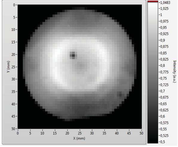
In the initial system qualification stage GaSb based bulk and GaInAsSb/AlGaAsSb quantum well structures were investigated. Experimental tests proved system robustness, reliability and performance for the intended application purposes. Numerous AlGaAsSb epitaxial structures were investigated after system qualification stage, for example PL intensity map of GaInAsSb/GaSb single quantum well (QW) structure is shown in Fig. 1. This PL intensity map and data mapping of other PL parameters (wavelength, FWHM) provide us valuable information about homogeneity of the epitaxial layer grown by MBE technique. Our experiments revealed that PL peak wavelength homogeneity across the wafer diameter is superior having less than 0.4% deviation providing great promise for industrial scale applications of the investigated structures.