
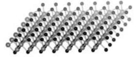
Two-dimensional materials are attractive for the application in nanoelectronic devices because of their extraordinary properties manifestation at the near atomic scales. Molybdenum disulfide (MoS2) is one of such materials. Monolayer of MoS2 (Fig. 1) has a direct band gap. Thus it can be used to construct interband tunnel FETs with lower power consumption than classical transistors. Monolayer MoS2 could also complement graphene in applications that require thin transparent semiconductors, such as optoelectronics and energy harvesting [1]. Further progress in understanding of physical phenomena at the nanoscale level may be realized by use of ab initio simulation [2] taking into account difficulties of experimental nanoobjects investigations.
This work is dedicated to the electronic and magnetic properties study of two-dimensional MoS2 structure with S- and Mo-vacancy clusters. Simulation was carried out by the means of the ab initio and molecular dynamics approaches realized in the program package VASP (Vienna Ab initio Simulation Program) [3]. The interaction between the ions and electrons in the simulated system is described by the Plane Augmented Waves (PAW) method. With the use of program package VASP it is possible to calculate the forces and stresses, which are used to relax atoms into their ground state. GGA-PBE pseudopotentials were applied for description of the interaction between the atomic cores and electrons. The calculations were performed using periodic conditions, therefore 4 × 4 supercell of MoS2, corresponding to 12.64 × 12.64 Å, was used to exclude the effect of vacancies on each other. In order to remove the interaction between MoS2 plates, vacuum gap of 10 Å was inserted between them. The sampling for Brillouin zone integrations is performed using the Gamma Scheme with a regular 4 × 4 × 1 k-point grid.
The results of densities of electron states (DOS) and energy bands calculation are presented (Fig. 2). Analysis of the calculated electronic properties and their dependences from the size and type of vacancy clusters are performed.
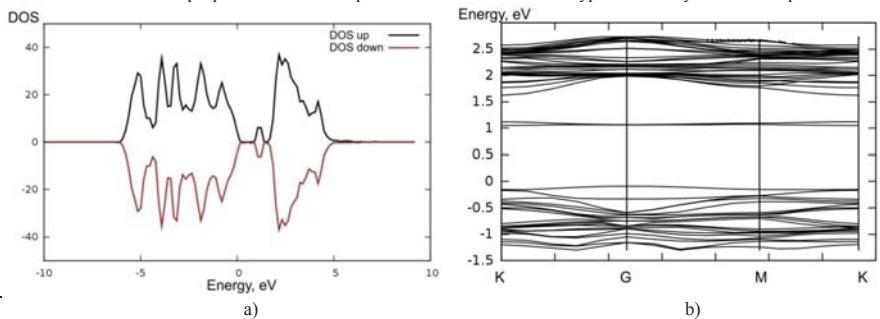
Analysis of the DOS and energy band calculations of the studied structures shows the appearance of additional energy levels in the band gap, which can be used as trap levels in laser technology. However, it's worth noting a slight change of the band gap value from 1.71 eV (perfect two-dimensional structure) to 1.64 eV with increasing S-vacancy cluster. While the Mo- vacancy cluster increase causes a sharp narrowing of the band gap to 0.11 eV and increasing of the magnetic moment value from $0.0008 \mu B$ (perfect two-dimensional structure) to $1.89 \mu B$. This fact suggests the possibility of using two-dimensional MoS2 as a structural element for sensors and spintronic devices.