
In these days ternary nitride compound, indium gallium nitride (InGaN) alloys are widely used in commercially available blue and white light-emitting diodes (LEDs) and light detectors [1]. The band gap of InGaN can be adjusted by changing the ratio of indium atoms to gallium atoms, that makes InGaN materials attractive for use in optoelectronics and photovoltaics. However, attempts to manufacture LEDs emitting light at longer wavelengths encounter problems due to increased defect density, high influence of internal electric field and carrier localization [2]. Some of the proposed ways to reduce these problems is using protective layers, ramping layers and quantum wells (QWs) with nonrectangular shapes.
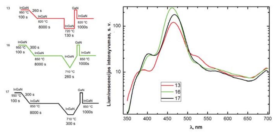
This work was focused on growth of InGaN multi quantum well structures on GaN templates grown on (0001) sapphire substrates by MOCVD method [3]. In order to improve quality of InGaN layer intermediate layered structures between GaN template and quantum wells were used. Many technological experiments were carried out to find best intermediate structure. The quality of the samples was estimated from photoluminescence measurements. The best results were obtained in samples with intermediate ramped layer (with In gradient) and prolonged first InGaN barrier with triangular-shape multi quantum wells (Fig. 1.).