In recent years, a lot of attention started shifting towards the investigation of point defects in view of their potential applications in quantum information processing. Nowadays, one of the most interesting defects is the NV center in diamond. Its quantum state can be optically initialized, manipulated, and measured with high fidelity at room temperature. Despite a big area of possible applications diamond has its technological shortcomings in real world applications, such as high costs and fabrication difficulties. Therefore, it is important to search for defects analogous to the diamond NV center in other wide-bandgap semiconductors [1].
In the last few years, hexagonal boron nitride (h-BN) has been attracting more attention with the emergence of two-dimensional atomic crystals and van der Waals heterostructures, initiated by the discovery of graphene. h-BN has one of the largest band gaps among III-V compounds. Its value was determined to be 5.955 eV by means of optical spectroscopy [2], so it is expected to host optically active defects that have ground and excited states within the gap. This year scientists were able to measure quantum emission from localized defects in h-BN monolayers and multilayers even at room temperature [3]. Another experiment shows possibility of manipulation of individual defects using scanning tunnelling microscopy [4]. However, it is still not clear what defects are a probable source of the measured emission.
Ab initio calculations, which are based on density functional theory (DFT), could bring a lot of valuable information about defects: they can predict whether a desired defect is likely to form in a given material and will be it stable once formed, etc.
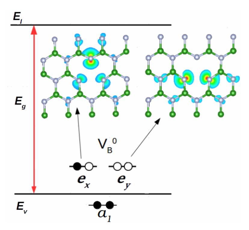
In this study we investigate boron vacancy, which is one of the dominating defects in h-BN. Boron vacancy defect has $C_{3\nu}$ point group symmetry. In neutral charge state, $V_B$ has 3 unsaturated dangling bonds. These defect states can be ionized by adding/removing electrons to it. Spin-polarized calculations were performed to examine neutral and positive charge states of this defect. Total spin states were determined and formation energies of these charged defects were calculated with ab-initio methods. Additionally first attempts to qualitatively estimate excited states were made. Detailed account of the results will be presented at the conference.