Scanning acoustic microscopy (SAM) is used as a routine non-destructive test tool for different diagnostic examinations: detection of defects such as micro-cracks, delamination, disbonding, inclusions, subsurface features in materials such as pores and cracks. SAM can be operated in a wide frequency range from MHz to GHz. SAM measurement spatial resolution is diffraction limited by the wavelength of the acoustic wave and also depends on particular transducers geometry. Actual SAM spatial resolution can be determine by measuring calibrated lithographically formed microstructures in high acoustic impedance materials [1-3].
Laser micromachining is an attractive one step lithography technique for producing micro structures. Micromachining with ultrashort pulses (nanosecond, picoseconds, femtosecond) provides additional advantages, such as high flexibility and very small heat-affected zones, since the short pulse duration results in high peak power intensities and the material is removed by vaporization, instead of melting as in long-pulse or continuous laser material processing [4].
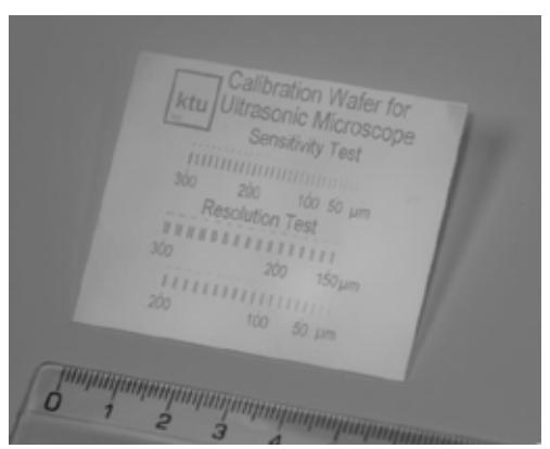
In this work the femtosecond laser micromachining technology that was applied to produce universal resolution and sensitivity calibration block for SAM is presented. Calibration block (Fig. 1) was micromachined in high acoustic impedance alumina ceramic substrates. Differently spaced (from 18 μm to 185 μm) lines of same widths and different widths (from 17 μm to 113 μm) but similar spacing lines were imposed in alumina ceramics employing Yb:KGW femtosecond laser ablation. The detailed analysis of the calibration block was performed employing optical and scanning electron microscopy as well as numerical simulation to show the feasibility of the device for calibration of SAM operating in a wide frequency range from 20 MHz to 230 MHz.