
When semiconductors such as GaAs, InAs or InGaAs are illuminated with femtosecond laser pulses, they emit electromagnetic waves in the range from 0.1 to 10 THz namely the Terahertz Gap. Such radiation is non-damaging, so it is attractive for medical uses or identification of explosives for safety purposes. Some molecules have distinct chemical 'fingerprint' in this region allowing their recognition in substances.
Generally, one of the main mechanisms contributing to terahertz generation is rapidly changing conductivity on a timescale of a few picoseconds. High currents are achieved by accelerating the photocarriers with external electric fields in the case of Photoconductive Antennas, however, a more technologically compelling solution would be to use intrinsic electric fields, which is the case for surface terahertz emitters.
It has been known for 11 years that the bulk p-InAs (1016 – 1017 cm-3) is the most efficient surface THz emitter [1]. p-InAs exhibits a natural surface charge accumulation due to high density of donor surface states which pin the Fermi level above its conduction band edge forming a space charge region. An analogy to this phenomenon are p-n or, more versatile, p-i-n junctions.
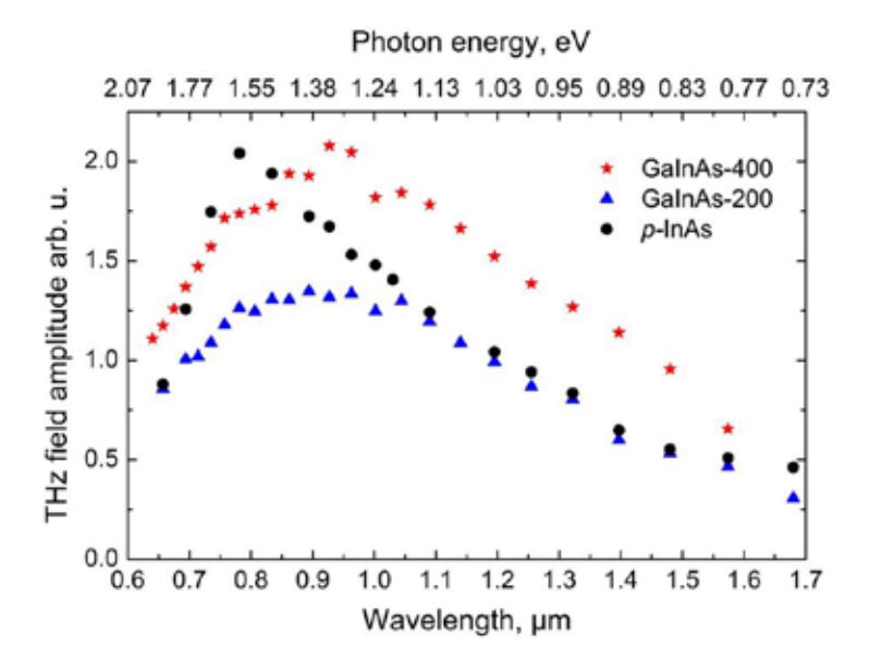
An InAs p-n junction has been MBE grown following an AlInAs buffer layer on an InP:S substrate. The thickness of n-type and p-type layers are 600 nm and 50 nm respectively. At wavelengths longer than ~1.8 μm the detected THz pulse amplitude is comparable to that of p-InAs. Two GaInAs p-i-n junction samples of different thicknesses of -i- i.e. 200 nm and 400 nm have also been grown. The p-type and n-type layers are of 50 nm of GaInAs:Be and 50 nm of GaInAs:Si respectively. From Fig. 1 it is seen that the THz field amplitude generated by the diode is ~75% larger than that obtained from the laser excited surface of the p-InAs single crystal [2].
Future goals are focused on investigation of InAs p-i-n structures.