
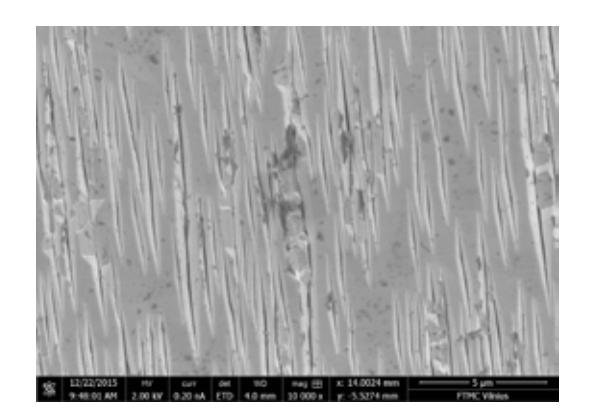
Recently, low-dimensional semiconductor nanomaterials in the forms of nanowires, nanorods, nanotubes, etc., have attracted great attention due to their potential for infrared optoelectronics and photovoltaic applications [1]. These nanomaterials also inspire potential applications in the terahertz (THz) range, for example, as an efficient terahertz emitters [2]. Despite the enhanced THz radiation efficiency, nanostructures like bulk semiconductors have the same limitation due to vertically oriented radiating dipole (i. e. the main part of the radiation propagates in parallel to the surface resulting in the low THz emissivity outside the sample). One way to overcome this problem is to use non-vertically aligned semiconductor nanowires as the electromagnetic dipole is oriented along the nanowire [3]. The other solution could be nanomaterials with more complex geometry or unusual physical properties. In the present work, THz emission from Ga-rich GaAs layer was investigated. It was found that excess gallium originates in submicron scale, elongated and oriented structures which determine unique properties of laser induced THz pulse emission from the layer (Fig. 1).
Investigated GaAs layer was grown by solid source molecular beam epitaxy (MBE) using SVTA reactor equipped with a metallic Ga and two-zone arsenic valved-cracker source to produce As2 dimers. The semi-insulating (100)-oriented GaAs wafers were used as substrates. GaAs layers were grown at a substrate temperature of 540°C and As2 and Ga beam equivalent pressure ratio close to 4. The thickness of GaAs layers was about 3.5 μm. Experiments have been performed using Ti:sapphire oscillator generating 150 fs, 800 nm pulses at the repetition rate of 76 MHz. THz electric field transients were detected with a low temperature grown GaAs antenna which was positioned to detect only p polarized THz radiation. THz emission measurements were carried out in transmission and quasi-reflection geometries. During measurements the samples were rotated around the normal to the sample surface – so called azimuthal dependencies were measured. Also THz pulse amplitude dependencies on an angle between the incident laser beam and a normal to the sample surface have been obtained.
In general, a laser beam induces two THz beams at the semiconductor surface: they propagate together with reflected or refracted laser beams. In the case of conventional semiconductor surfaces the intensity ratio between both THz beams is constant regardless of the azimuthal angle. In this context, our investigated sample demonstrates anomalous behavior: depending on the azimuthal angle, THz energy apparently passes between reflection and transmission modes (Fig 2).
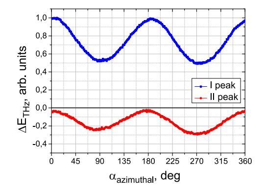
Such behavior we explain by coexistence of two types of radiating dipoles. Perpendicular to the semiconductor surface dipoles are typical for semiconductor surface emitters, whereas parallel dipoles are very effective and preferable but hardly realizable. Our results demonstrate that nanostructuring of semiconductor surfaces leads to the appearance of the electric fields which force photoexcited carriers to move parallel to the surface. Moreover we introduce measurement techniques which allows us to observe and analyse the generated fields.