
Controllable fabrication of Si nano and microstructures has a lot of practical applications in functional devises fabrication. A big range of methods have been developed to fabricate Si nanostructures, such as vapor-liquid-solid (VLS) growth, reactive ion etching (RIE), electrochemical etching or metal-assisted chemical etching (MACE), all of which aim to control various parameters of the Si structures in functional devices [1]. Metal-assisted chemical etching method uses a thin layer of noble metal (e.g., Au, Pt, or Au/Pd alloy) sputtered on the surface of a Si substrate that catalyzed the etching of Si in a mixed solution containing HF, H2O2, and EtOH, resulting in straight pores or columnar structures. Furthermore, as MACE is based on a simple redox process in an etching solution, it produces a very smooth and clean Si surface that is free of the surface damage that typically results when using the RIE process [2]. However high noble metals cost is limiting factor for practical applications and cost reduction with use of cheaper metals is serious task to achieve.
In this work we present nickel (Ni) assisted etching for silicon. Commercially available p-type (100) 1-5 Ohmcm wafers were used. For the investigations Ni layers with different thickness were deposited by magnetron sputtering and electroless plating. Test structures were formed by using lithography and Ni etching in acid solutions for samples with thin magnetron sputtered layers and by electroless plating on opened areas in photoresist by lithography. Silicon etching was carried by immersing samples in HF:H2O2:H2O solution. After etching samples were investigated using atomic force microscopy (AFM) (fig. 1). From AFM images statistical investigations on etched structures was made by using SPIP software.
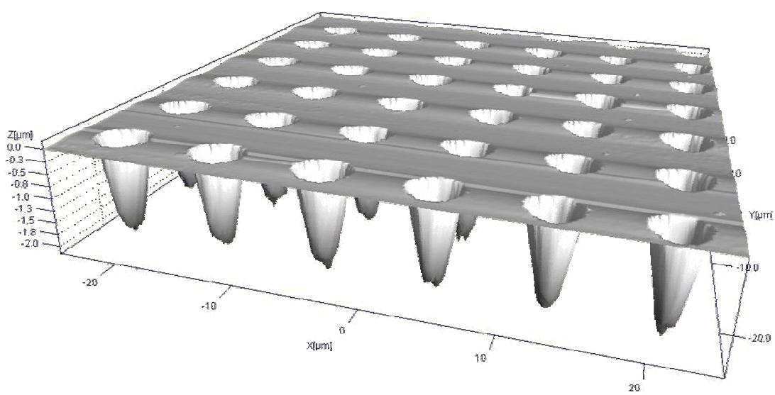
Influence on technological parameters (Ni layer thickness, etching time, etchant ratio) for etched structures was investigated.