Group-III nitrides are widely used for optoelectronic devices such as light emitting diodes and laser diodes. However, most epitaxial nitride layers are grown on foreign substrates such as sapphire and silicon carbide because native ones are currently expensive. One problem associated with III-nitrides is spontaneous polarisation that appears when growing along c-direction, due to the lack of inversion symmetry in hexagonal crystal structure. This leads to energy band bending and efficiency decrease as well as spectral instability of LEDs. Silicon (100) substrates are suitable for gallium nitride (GaN) growth in non-polar and semi-polar directions. Rear-earth oxide interlayers could be used to solve problems related to high lattice mismatch, thermal expansion coefficient differences as well as to prevent gallium reactions with silicon.
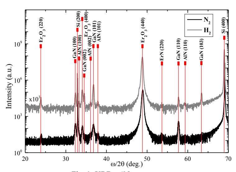
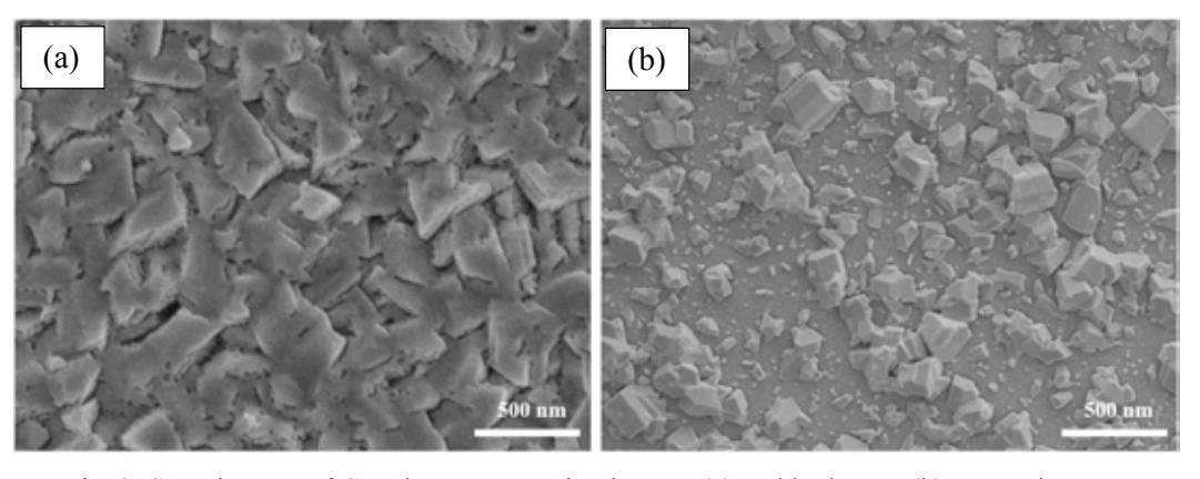
We have used slightly miscut Si (100) substrates coated with 300 nm erbium oxide (Er2O3) interlayers for GaN heteroepitaxy. The aim of this work was to find optimal growth conditions for GaN formation in non-polar directions. Growth of III-nitrides was performed in close-coupled showerhead metalorganic chemical vapour deposition reactor (MOCVD). Growth conditions such as temperature, V/III ratio and carrier gases were varied. Aluminium nitride (AlN) interlayers as well as various GaN layers were used for stress management. Grown epitaxial structures were investigated using X-ray diffraction (XRD), scanning electron microscopy (SEM) and photoluminescence (PL) techniques. Investigation of grown structures showed that nitrogen atmosphere during GaN growth prevents it from forming towards polar [001] direction as well as helps to obtain smoother epitaxial layers (Fig. 1). In hydrogen atmosphere polycrystalline island-like GaN growth was observed (Fig. 2).