
Synthetic diamond and GaN are promising wide band-gap materials for fabrication of the solar-blind photosensors and radiation tolerant particle detectors applied in high energy physics, radiation monitoring and other fields [1,2]. Wide band-gap determines low leakage current and proper radiation hardness of devices made of these materials. High carrier mobility determines fast charge collection of devices made of diamond. High luminescence efficiency is an attractive characteristic of GaN. Diamond and GaN materials of large thickness (300-600 μm) and high resistivity (≥106 Ωcm) can also be used for manufacturing of the capacitor type particle sensors with high sensitivity [3]. Diamond crystals of such thickness can be synthesised by high pressure and high temperature (HPHT) while GaN – by hydride vapour phase epitaxy (HVPE) and ammono-thermal (AT) techniques. Additionally, acceptor type impurities are often introduced during growth of GaN to reach high resistivity of the material. However, technological defects and impurities introduced during crystal growth process affect functional characteristics of devices made of diamond and GaN materials. The knowledge of parameters of the technological defects is very important in prediction of operational characteristics (leakage current determined by recombination defects, charge collection efficiency affected by trapping centres, etc.) of detectors, and the spectroscopic methods are highly effective tools for the investigation of these defects.
In this work electron spin resonance (ESR) technique has been applied for characterisation of defects and impurities introduced in HPHT diamond, HVPE and AT grown GaN samples during the growth process. Four diamond wafer samples with surface normal being of <001> direction and two GaN wafer samples of HVPE and AT grown technology with surface normal being parallel to hexagonal lattice c axis have been investigated. Measurements were performed in the temperature range of 100-300 K using Bruker Elexsys E580 spectrometer.
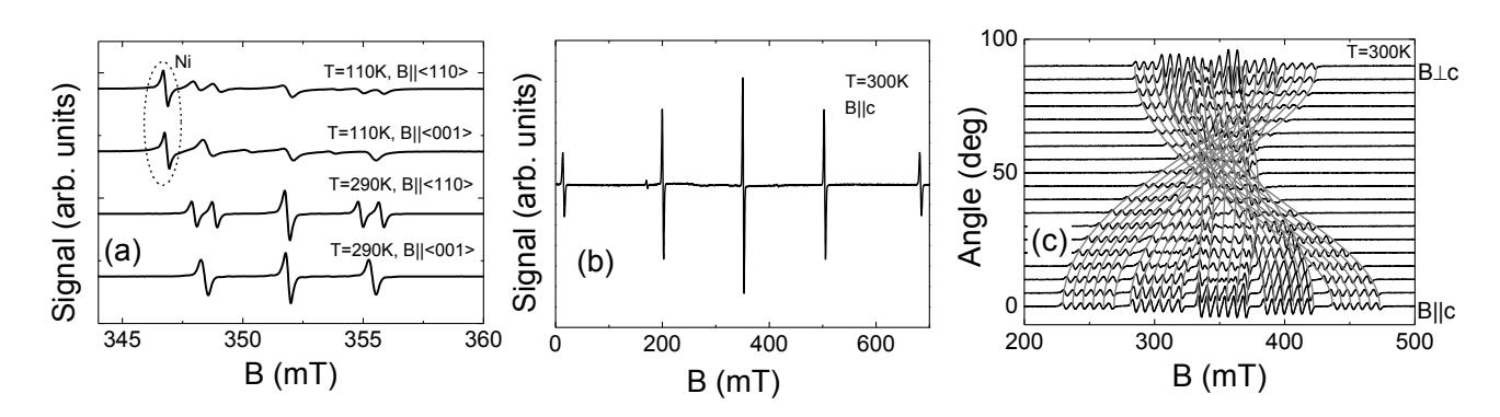
Analysis of ESR spectra measured at different temperatures and microwave power levels, as well as using different magnetic field orientations relative to crystal axis (Figure 1) allowed us to determine the spin-Hamiltonian parameters of spin system and to identify the dominant spin-active defects and impurities in materials under investigation. The density of defects has been evaluated using Bruker software. Substitutional nitrogen and substitutional negatively charged nickel (Nis-) paramagnetic centres ascribed to P1 and W8 defects, respectively, have been identified in HPHT diamond samples. Densities of the predominant paramagnetic impurities in HPHT single crystal diamond wafer samples were evaluated to be up to $2 \times 10^{19}$ cm-3 and $2 \times 10^{17}$ cm-3 of nitrogen and of nickel impurities, respectively. In the HVPE grown semi-insulating GaN samples the intentionally introduced Fe3+ impurities have been detected and concentration of $2 \times 10^{17}$ cm-3 has been evaluated. Meanwhile, Mn2+ impurities have been identified in the AT grown GaN sample. The concentration of Mn2+ impurities has been evaluated to be of $10^{19}$ cm-3. The analysis of the ESR spectra and procedure for identification of spin-active defects and impurities will be discussed.