The main purpose of GaN buffer in any nitride-based heterostructure is reduction of lattice strain and damping of threading dislocations. Both functions decrease the defect density in upper layers and increase overall quality of the heterostructure, implying that the quality of all subsequent layers is determined by an underlying layer. In this report, I demonstrate a reverse effect – the influence upper layer has to base layer properties.
For the study, a set consisting of eleven 130 – 300 nm thick AlGaN epilayers was grown using metalorganic chemical vapor deposition (MOCVD) on c-plane GaN/sapphire templates. GaN buffer for every sample was grown at identical conditions, and initially was of the same quality. Al content x in AlxGa1-xN epilayers varied from 11% to 28%, as determined from XRD measurements. Nonradiative carrier lifetime was used as a measure of quality, and was extracted from kinetics of light induced transient gratings (LITG). 25 ps duration pulses of 263 nm and 355 nm wavelength were used for excitation of AlGaN epilayers and GaN buffers, respectively.
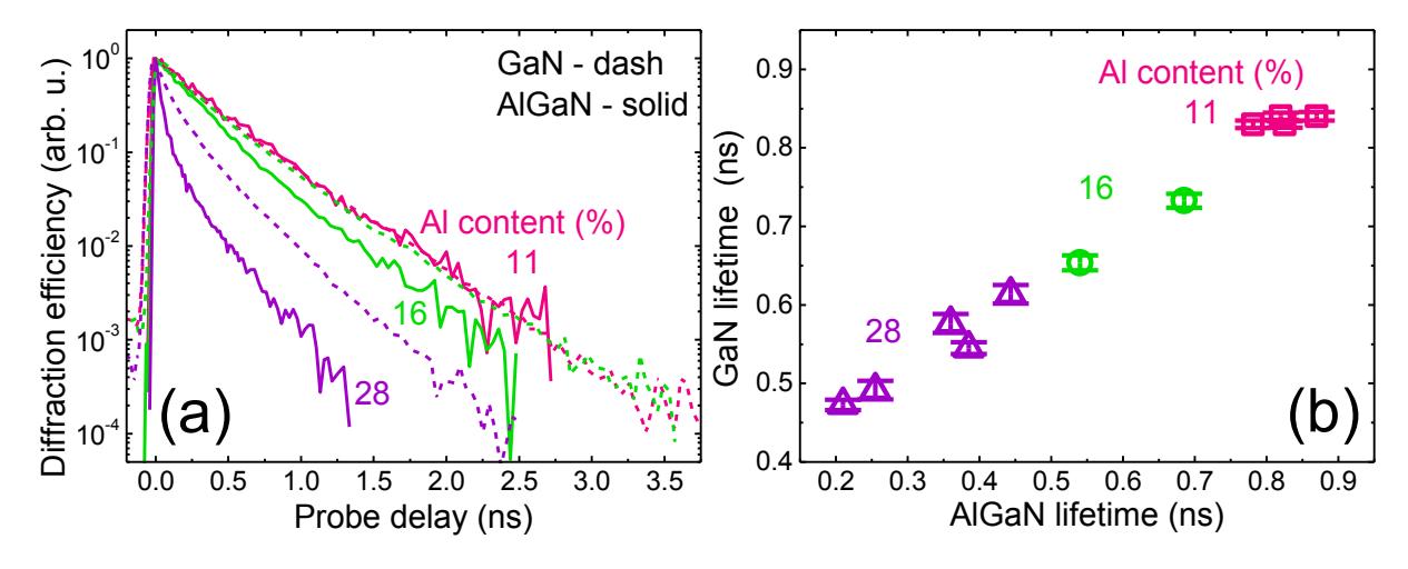
Analysis of LITG results indicated that nonradiative carrier lifetime $τ$ in AlGaN epilayers was strongly influenced by Al content $x$: $τ$ decreased from 0.9 to 0.2 ns with increasing $x$ (see solid lines in Fig. 1. (a) and abscissa axis of Fig. 1. (b)). This outcome could be determined by two processes: (i) deterioration of crystal quality (increasing density of nonradiative centers); (ii) increasing carrier diffusivity $D$ (from 1.2 to 2.3 cm2/s with increasing $x$). Carrier diffusivity can govern their lifetime since carriers have to diffuse to nonradiative centers to recombine. Meanwhile, diffusivity can increase with Al content due to interchange of upper valence subbands: crystal field band CH of lower effective mass emerges above heavy holes band HH ($m_{HH}$ = 3.57$m_0$, $m_{CH}$ = 0.26$m_0$) at $x$ = 0.04 – 0.6 (depending on strain).
Carrier lifetime measurements in GaN buffer revealed unconventional $τ$ variation from sample to sample in the range of $τ$ = 0.5 – 0.9 ns (see dashed lines in Fig. 1. (a) and ordinate axis of Fig. 1. (b)). This result should not be expected since GaN buffers in every sample were grown at identical conditions. The correlation between carrier lifetimes in GaN and AlGaN layers (Fig. 1. (b)) implies that during the growth, defects of AlGaN penetrated interface of AlGaN/GaN and deteriorated the very surface of GaN buffer at that interface. This result is particularly important in development of AlGaN/GaN high-electron-mobility transistors (HEMTs), since underlying GaN layer in HEMT determines the performance of a whole device.