Silicon Carbide (SiC) and its polytypes are of huge interest for power and opto-electronic devices. SiC has a unique combination of physical and chemical properties: a wide bandgap, attractive thermal and chemical properties, elevated electron drift velocity and high break-down voltage. On the other hand, SiC substrates are too expensive for commercial mass-production, therefore the development of the methods for defect-free epitaxial growth of SiC layers on the Si substrates is of great necessity. The task of SiC-on-Si growth is very complex because Si and SiC have different thermal expansion coefficients and there is a significant lattice misfit [1-2]. Another reason for defects in hetero-epitaxial SiC is the presence of SiO2 islands on the surface of Si-substrate [3]. These islands might be removed by interaction with hydrogen atoms during thermal treatment in vacuum [3]. In addition, high-temperature treatment in hydrogen-containing vacuum is expected to saturate surface layer with hydrogen atoms resulting in modification of lattice parameters and reduction of structural defects. Therefore, in this work we used hydrogen treatment of Si substrate to make it relevant for the growth of thin epitaxial SiC layers.
The (100) Si wafers are used in this study. Just before high-temperature processing in a vacuum chamber, the samples are chemically cleaned and their surface is refreshed in 5% HF+H2O solution. Thermal treatment of the samples and the growth of SiC layer is proceeded in a tungsten-foil-based heating cell. The cell is constructed in a vacuum chamber and is equiped with a thermocouple and two gas inputs. The process is carried out in four stages. At the first stage the chamber was evacuated to 1·10-3 Pa. After that the hydrogen is injected up to a vacuum of 8 · 10-3 Pa and the samples are heated to 700 °C for 10 min. At the third stage the temperature is increased and the carbon containing gas is injected to the heating cell. The growth of SiC layers takes place at the fourth stage and the process is carried out at 1100°C for 10 min in a vacuum better than 1·10-3 Pa.
The structure of Si/SiC layers is finally studied by scanning electron microscopy (SEM), transmission electron microscopy (TEM), and transmission electron diffraction (TED). The LEO 1455VP and TEM Hitachi H-800 devices are used for SEM and TEM investigations respectively. The samples are prepared for TEM study by using routine chemical etching from the back side.
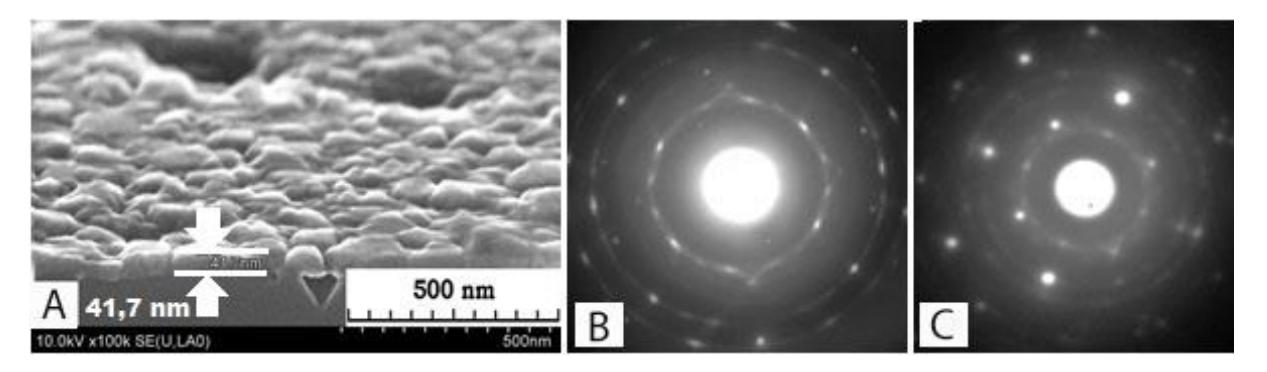
Fig. 1 shows representative SEM image and TED patterns of SiC layers grown on different Si substrates at 1100°C for 10 min. Comparison of diffraction spots indicates an improvement in the structural quality of SiC layers grown on a substrate treated in a hydrogen-enriched atmosphere. SEM investigations shows (Fig 1a) that the SiC layer is about 40 nm thick and the surface is rough due to nanometer-size pores in the Si substrate. The mechanisms of the growth is discussed taking into account chemical reactions on the surface and Kirkendall assisted pore formation in the Si substrate.