
Silicon sensors with charge multiplication layer, known as Low Gain Avalanche Detectors (LGAD), are anticipated to be the functional particle detectors after heavy irradiations by hadrons. The concept of internal gain due to charge multiplication is addressed to an enhancement of the signal-to-noise ratio (SNR). The LGAD detectors become the most promising devices for applications in high energy physics experiments where harsh radiation environments, such as the inner detectors of Large Hadron Collider (LHC), are met.
Conventional a P-type LGAD consists of N+PP-P+ layers with P-well formed by deep diffusion of boron (B) into P-layer. However, it was shown that an effect of the "acceptor removal" occurs in irradiated LGAD sensors which causes the loss of internal gain [1]. Radiation damage partially removes a boron from the multiplication layer, thereby reducing the effective doping concentration. Acceptor removal is consistently described by relation:
$$N(\Phi) = N_0 \cdot e^{-b\Phi},\tag{1}$$where N is the dopant concentration (acceptor density), $\Phi$ is the irradiation fluence, and the parameter b which is a function of N0. This detrimental effect might be partially suppressed by forming the N-well (P+NN-N+) Si structure with the phosphorus doped an epitaxial (N-well) layer. In this work, the results of simulations of the operation characteristics for the P-type and N-type LGAD devices are reported.
A functionality of LGAD device has been validated by digital experiments performed using of Technology Computer-Aided Design (TCAD) algorithms and the Drift-Diffusion (DD) approach. Simulations have been carried out employing a Sentaurus Device software platform. It has been obtained that the shape and duration of current pulses is quite different (Fig. 1) in N- and P-type Si LGAD's mainly due to the difference of the ionization coefficients. These coefficients are approximately 10 times greater for electrons than for holes ($\alpha_e \cong 10 \cdot \alpha_h$). Nevertheless, the collected charge is almost the same for P-type (Fig. 1a) and N-type (Fig. 1b) Si devices if radiation traps are ignored in simulations.
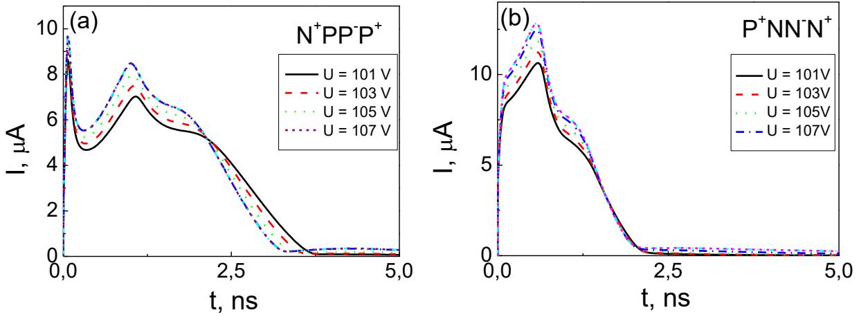
A probability of carrier trapping during their drift increases with irradiation fluences assumed in simulations. It has been shown that thickness of the active layer within a sensor plays an important role in charge collection. Nevertheless, the rather thin (~50 μm) modelled LGAD sensors appear to be functional and exhibit a proper charge collection efficiency due to the carrier density increase through the internal amplification, proportional to the radiation injected secondary carrier pairs. It has been demonstrated that the rather low bias voltage, applied to LGAD, is sufficient to get proper charge collection. The impact of radiation induced traps which affect the detector current and charge collection efficiency will be discussed.