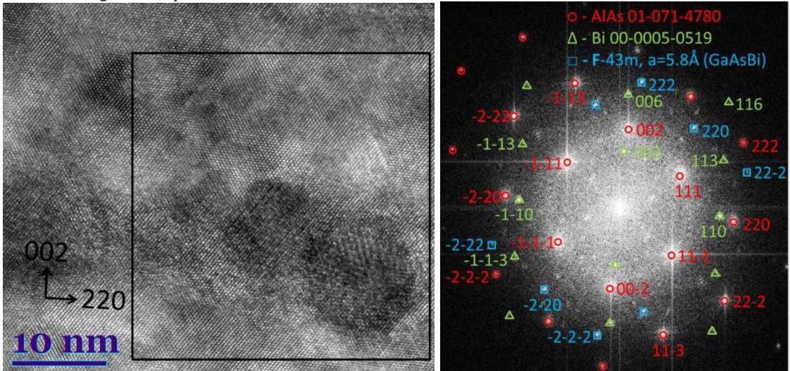
High Resolution Transmission Electron Microscopy (HRTEM) is the premier tool for understanding of the internal microstructure of materials at nanometer level. This method allows to distinguish real-space nano-scale peculiarities in material, and simultaneously from Fast Fourier Transform (FFT) diffraction patterns obtain the information about crystalline lattice of the investigated specific regions in the nanostructures, such us, nanoparticles, quantum dots, and etc.
In this work, MBE grown and thermally treated GaAsBi/AlAs quantum wells were studied by structural (High-Resolution X-ray Diffraction, HRTEM) and optical (PL) characterizations. The analysis of profile of GaAsBi/AlAs QWs containing Bi-nanoparticles measured by HRTEM and Scanning Transmission Electron Microscopy in High-Angle Annular Dark-Field (STEM HAADF) mode were performed to evaluate the influence of annealing on orientation of nanoparticles and strain distribution in whole quantum structure. Energy Dispersive X-ray Spectroscopy (EDS) mapping and STEM HAADF revealed re-distribution of Bi atoms in GaAsBi quantum wells during high temperature annealing and formation of semiconducting Bi nanoparticles in the wells of GaAsBi with lower Bi content. The significant changes in crystalline lattice of GaAsBi quantum wells were shown by HRXRD ${\omega}$-20 scans. Also, the PL measurements demonstrated the additional low-energy peak appeared in the spectra after thermal treating, and attributed to semiconducting Bi-nanoparticles.