
AIII-BV group compounds are attractive due to their wide applications in optoelectronics. GaInAs compound lattice-matched to InP for a quite long time was suitable for optoelectronics devices operating in telecommunications "windows" and in near-infrared region up to ~1.7 µm wavelengths. Dilution of GaInAs by Bi could lead to engineering of good alternative compound for longer wavelengths applications. It was demonstrated that even low content of Bi can considerably reduce the bandgap (Eg) of semiconductor. Moreover, the conditions for epitaxial growth of lattice-matched GaInAsBi to InP substrate can be realized by optimization of In and Ga ratio as well Bi content. Theoretically the working range of such GaInAsBi/InP systems can reach 6 µm [1].
In this work, thick GaInAsBi epitaxial layers were grown by molecular beam epitaxy (MBE) on semi-insulating (100)-oriented InP:Fe substrates with GaInAs buffer layer. The buffer layer thickness varied from 100 nm to 650 nm. Two compositions of buffers were used: lattice-matched to InP:Fe substrate and lattice-matched to bismide layer. 300 nm thick bismide layers were grown at 280°C-300°C substrate temperature with growth rate of 300 nm/h. Two different flux ratios of In/Ga were kept for GaInAsBi layers growth on different buffer layers. The Bi/Ga flux ratio in both cases varied in order to introduce the larger content of bismuth and fulfil the conditions of lattice-matching of buffer and bismide in-plane. The effect of the annealing on structure and optical characteristics of quaternary GaInAsBi alloy were investigated. Layers were annealed at rapid thermal annealing oven for 180 s at temperatures ranging from 450°C to 750°C.
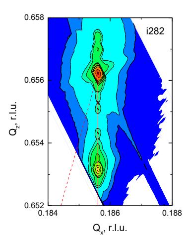
For evaluation of structural quality the $\omega$-20 rocking curves of (004) reflex and reciprocal space mappings (RSM) of (115) reflex were measured and analysed. The modelling of measured rocking curves allowed estimating the incorporation of Bi up to 3.6% in quaternary compound lattice. The reciprocal space mapping measurements demonstrated that both buffer and the bismide layers are fully strained (Fig. 1).
Both annealed and as-grown GaInAsBi layers were characterized by optical absorption, photomodulated reflectance, photoluminescence (PL) measurements. The carrier lifetimes were determined from the optical pump – THz probe measurements. Complex study of GaInAsBi properties showed an improvement of optical characteristics. It was found that rapid thermal annealing at temperatures in the range of 650-700°C improves photoluminescence intensity, extends carrier lifetime and enhances electron mobility. Strong PL signals at longer than 2.2 µm light wavelengths and relatively long lifetimes evidence that this quaternary compound could be prospective for IR optoelectronic applications.