
THz detection based on resistive mixing and enhanced by plasmonic effects at high frequencies is an important feature in the THz photonics field [1, 2]. Until now, the highest sensitivity has been reached with silicon CMOS devices with narrow-band antennas, which exhibit an optical noise-equivalent power (NEP) of ≥10 $pW/\sqrt{Hz}$ [3]. To improve robustness against electrostatic shock, which is a crucial aspect in many applications, as well for a multiple-pixel array, we use III-V group materials, namely GaN/AlGaN HEMTs, for an effective THz detection [4]. After an extensive optimization effort on the single device fabrication technology and the device design, published in [5, 6], here we present the device characterization and sensitivity enhancement at low temperatures.
GaN/AlGaN TeraFETs were developed to work with various types of integrated broadband antennas and substrate-side radiation coupling. The best performance is achieved with FETs with integrated bow-tie antenna. These devices have a gate width of 3 μm, a channel length of 900 nm, and a small gated-channel length of only 100 nm, which is possible by advances of the fabrication technology.
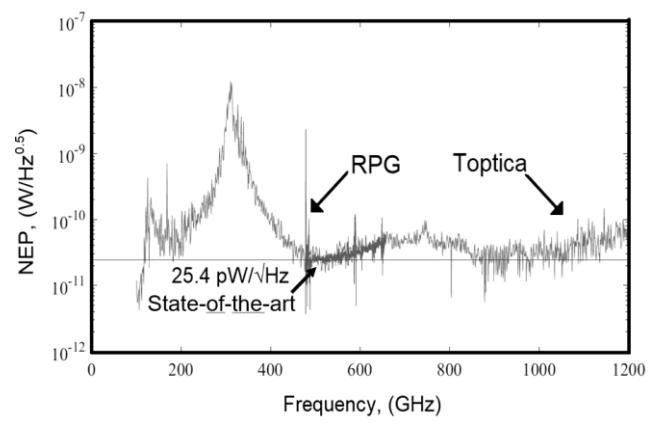
The room-temperature optical NEP of these TeraFETs was measured at frequencies from 0.1 THz to 1.2 THz with a Toptica TeraScan 1550 system and a RPG radiation source. The data for the two different sources are compared with each other in figure 1. At room temperature, we determine a state-of-the-art optical NEP for quasi-optical detectors of 25.4 $pW/\sqrt{Hz}$ at 490 GHz. The maximum current responsivity RI reaches 104 mA/W. These values are usually achieved only with narrow-band antennas in other material systems. Concerning these key quantities, GaN/AlGaN TeraFETs are now competitive with Si CMOS room-temperature THz detectors.
Further characterization of GaN/AlGaN TeraFETs proved the noise limitation to be given only by thermal noise as it is the case also for other material systems. Upon cryogenic cooling of a device, we observed an improvement of the best NEP by a factor of 13.8 and of the maximum current responsivity by a factor of 3.8 at 630 GHz at liquid nitrogen temperature. Measurements at cryogenic temperatures enable us also to adapt the Dyakonov-Shur responsivity formula for real devices and to use this advanced device model as the main tool for the extraction of internal device parameters needed for further device improvement. From such devices, we have already built a 12 x 12 pixel integrated array for a camera implementation.