
Ultrathin metal films play an important role in the nowadays micro- and nanoelectronics, optoelectronics and photonics. Cu thin films are well known because of two important characterizations: high electrical conductivity and high electro-migration resistance. Nevertheless, in recent years due to nonlinear optical properties change some new applications in optics appear. The reason is that copper may represent discontinuous, island-like structures that exhibit excitation of localized plasmon–polaritons under light illumination.
It is essential to find optimized deposition conditions and be able to tune effectively optical properties of prepared material. For this reason in this work, copper films growth is investigated in details. Copper, as other noble metals (gold, silver and etc.), has distinctive growth stages when growing on dielectric substrates (3D Volmer-Weber growth mechanism). Optical properties of during such growth highly depend on the structure of the film.
Copper films were prepared by magnetron sputtering technique. In-situ real-time measurements of transmittance spectra change during growth of the film were done (Fig. 1). Three stages of copper film growth depending on layer thickness were determined from these measurements.
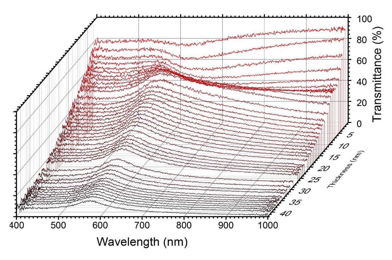
Moreover, five samples of different thickness were prepared, their transmittance, reflectance spectra were measured and losses values were calculated. Measured and calculated data were compared with theoretical values for continuous copper films.