The wide band gap Gallium nitride is an excellent semiconductor for the production of high power, high speed transistors [1] as well as semiconductor lasers [2] and light emitting diodes (LEDs) [3]. While GaN bulk substrates are still too expensive for practical use, much attention is drawn towards GaN on Si technology. However, in case of heteroepitaxy, technical difficulties arise due to the difference of crystal lattice types and constants together with thermal expansion coefficients between these two substances. In order to grow high quality GaN, an interlayer of Er2O3 could be used to reduce the lattice and thermal mismatch between Si and GaN [4]. Moreover, to avoid the cracking of GaN, it can be grown on a patterned substrate [3].
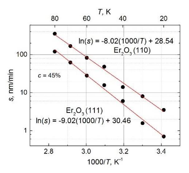
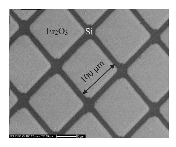
In this work the wet etching process was investigated in order to perform patterning of Er2O3 films on Si using photolithography. Etching rates and activation energies in H2SO4 and HCl were evaluated. The layers of Er2O3 were patterned as well as the size of the etched structures was determined. Finally, the influence of diffusion and the anisotropy of etching speed are discussed.