
Development of technologies for organised nanoscale structures are demanding due to applications in fluid dynamics, sensors or optical devices. Periodic structures in noble metal films are particularly interesting due to their plasmonic properties [1]. Silver nanoparticles based plasmonic structures can be fabricated in many different approaches, e.g. evaporation, sputtering, ion implantation [2]. Another approach is laser irradiation, which leads to formation of nanoislands, beads, nanoparticles or self-organised patterns [3]. In order to further control optical properties of plasmonic material, it can be embedded in dielectric or semiconducting matrix. This is also beneficial for protecting nanoparticles from unwanted degradation in environment [4].
In this work, we present laser interference field ablation of amorphous diamond-like carbon (DLC), silver (Ag) and nanocomposite (DLC:Ag) thin films on silicon and quartz substrates. DLC and DLC:Ag films were fabricated employing magnetron sputtering in a mixture of acetylene and argon gas using carbon and silver targets, respectively. Ag films were fabricated by e-beam evaporation. The thickness of deposited films was 60 nm.
One-dimensional (1D) periodic structures in thin films were ablated using Yb:KGW femtosecond laser pulses (second harmonic wavelength 515 nm, pulse duration 290 fs). The laser beam was separated into two using diffractive optical element (DOE) and then overlapped with 4f lens system into one spot on the surface of the sample to create the interference pattern. The pitch of the pattern was altered by changing the angle of the incidence, i.e. changing the pitch of the DOE. To find best parameters of microfabrication the laser fluence was varied from 1 mJ/cm2 to 226 mJ/cm2 and the number of applied pulses was varied from 1,000 to 125,000. The total area of ablated pattern was 300 × 300 μm2. For each pitch, the total of 25 patterns with different micromachining parameters were created.
The ablated structures were investigated using scanning electron microscope (SEM, Hitachi S-4800) and helium ion microscope (HIM, Zeiss ORION NanoFab) (Fig. 1). The determined pitches of 1D structures are 1.26 μm and 0.56 μm.
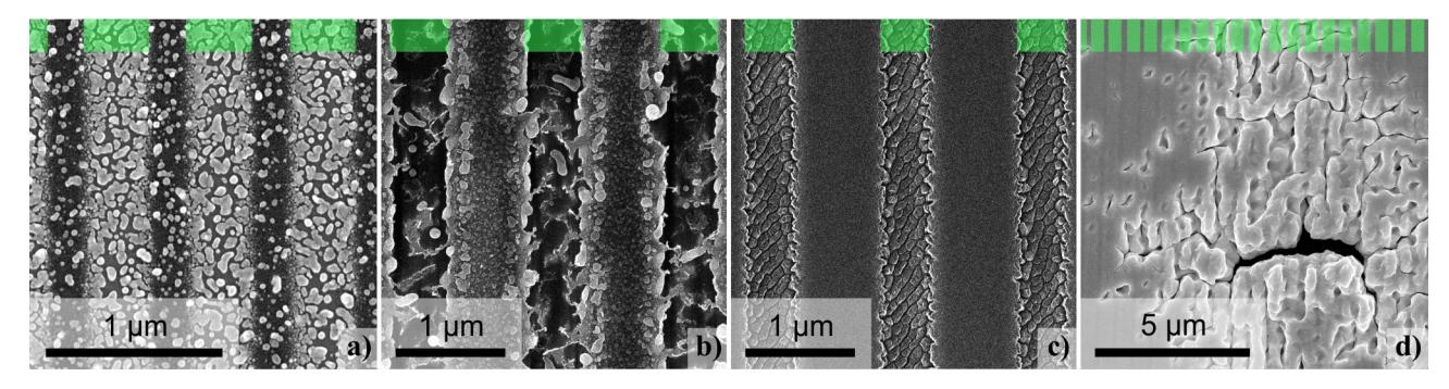
From the microscopy characterisation it was determined that ablation threshold is lower for composite DLC:Ag materials than pure DLC or Ag. For DLC:Ag with higher silver content the laser fluence should be at least 10 mJ/cm2 together with 64,000 pulses, while for lower silver content the structure is already present with 27,000 pulses at the same fluence. For DLC the fluence should be at least 27 mJ/cm2 with 8,000 pulses. For Ag the fluence should be at least 145 mJ/cm2 with 64,000 pulses, however this results in a damage of the film rather than 1D structure. In all cases, for higher fluences the number of pulses can be decreased. Only for pure Ag increasing the fluence even more results in the peeling off of the film. In conclusion, femtosecond laser interference field ablation is convenient tool for fabrication of 1D periodical structures in various materials, if the laser parameters are carefully selected.