Low Gain Avalanche Detector (LGAD) is the perspective technology used in ATLAS and CMS detectors due to their high-precision timing performance. However, their highly boron-doped gain layer is susceptible to radiation-induced deactivation of boron dopants, known as the Acceptor Removal Effect [1]. Understanding boron-associated deep-level defects is crucial for ensuring the reliable operation of these detectors in harsh radiation environments.
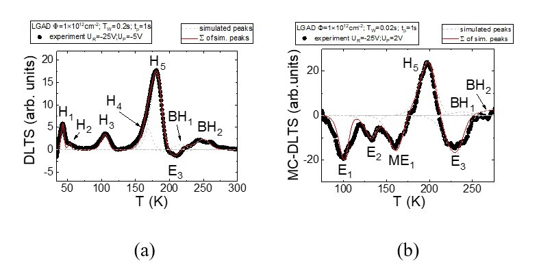
In this study, Deep Level Transient Spectroscopy (DLTS) and Minority Carrier Deep Level Transient Spectroscopy (MC-DLTS) were performed on p-type LGAD and PIN detector samples irradiated with 26 GeV protons at a fluence of 1×10\(^{12}\) cm\(^{-2}\). Trap analysis was conducted using correlation functions, Laplace transformation, and literature references [2–4]. The DLTS spectra revealed up to seven hole traps (H), as shown in Figure 1a, while the MC-DLTS spectra exhibited up to four electron traps (E), as shown in Figure 1b.
Fig. 1. (a) the DLT and (b) the MC-DLT spectra recorded on the irradiated LGAD sample.
ME\(_{1}\) trap is a metastable defect, and it can disappear after forward current (electron injection) and BH\(_{1}\) and BH\(_{2}\) traps can appear. After annealing, this process is backward, which means that the metastable ME\(_{1}\) trap (negative-U center) is connected with BH\(_{1}\) and BH\(_{2}\) traps, and they all belong to the same DBH defect. Boron atoms take part in the formation of the DBH defect [4]. The traps of E\(_{1}\) and E\(_{3}\) are usually not represented in the MC-DLT spectrum of p-type Si diode (it is more common for n-type Si majority traps). Still, they can be “highlighted” in p-type semiconductors by using optical Minority Carrier Transient Spectroscopy [5]. In our case, we have several layered structures (LGAD), which can pull minority carriers from another layer.
While previous DLTS studies have focused on PIN diodes, the application of DLTS to LGADs provides new insights into the formation of radiation-induced defects in these p-type structures. This research enhances our understanding of carrier recombination processes in avalanche diode layers, contributing to the development of more radiation-tolerant detectors.
[1] A. Himmerlich, N. Castello-Mor, E. C. Rivera, Y. Gurimskaya, V. Maulerova-Subert, M. Moll, I. Pintilie, E. Fretwurst, C. Liao, J. Schwandt. Defect characterization studies on irradiated boron-doped silicon pad diodes and Low Gain Avalanche Detectors. Nuclear Inst. And Methods in physics Reseach, A 2023, 1048, 167977.
[2] T. Ceponis; S. Lastovskii; L. Makarenko; J. Pavlov; K. Pukas; E. Gaubas. Study of radiation-induced defects in p-Type Si1-xGex diodes before and after annealing. Materials 2020, 13, 5684.
[3] J. Pavlov; T. Ceponis; K. Pukas; L. Makarenko; E. Gaubas. 5.5 MeV electron irradiation-induce transformation of minority carrier traps in p-type Si and Si1-xGex alloys. Materials 2022, 15, 1861.
[4] L.F. Makarenko; S.B. Lastovski; H. S. Yakushevich; E. Gaubas; J. Pavlov; V.V. Kozlovski; M. Moll; I. Pintilie. Formation of a bistable interstitial complex in irradiated p-type silicon. Phys. Status Solidi A 2019, 216, 1900354.
[5] P. Blood; J.W. Orton. The electrical characterization of semiconductors: majority carriers and electron states. Academic Press Inc.: San Diego, CA, USA, 1992.