Indium gallium nitride (InGaN) - a ternary nitride compound - alloys are now widely used in commercially available blue and white light-emitting diodes (LEDs) and light detectors [1]. What makes InGaN materials attractive for their use in optoelectronics and photovoltaics is an ability to adjust their band gap by changing the ratio of indium atoms to gallium atoms. Attempts to manufacture LEDs emitting light at longer wavelength are problematic due to increased defect density, high influence of internal electric field and carrier localization. To improve the effectiveness of these structures and to develop green emitters, a more sophisticated design of the structure is required, which leads to a more complex dependence of LED parameters on the growth conditions. One of the proposed ways to reduce these problems is to use short-period InGaN/GaN superlattice (SPSL) structure in the buffer area [2].
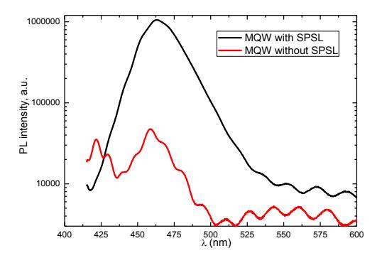
The main objective of this work was to grow high quality blue InxGa1-xN multiple quantum wells (MQWs) on GaN templates previously grown on (0001) sapphire substrates by MOCVD method. In order to reduce the resulting lattice strain – an often encountered problem – the interlayer between buffer layer and active region with InGaN/GaN SPSL was formed by changing the flow of trimethylindium metalorganic, but keeping flow of other precursors and growth temperature constant. Multiple experiments were carried out to find the best SPSL structure. Some samples investigated by X- ray diffraction measurements; the quality of grown samples was estimated by photoluminescence (PL) and atomic force microscopy measurements. The best results were obtained in samples with 8 period InGaN/GaN SPSL, where InGaN layer width of 1.7 nm and concentration of In ~ 6%, GaN layer width 2.2 nm. It is shown, that using InGaN/GaN SPSL structure, MQWs PL intensity at 450nm wavelength increase ~22 times in compare with the structure without SPSL (Fig. 1). However, SPSL layer increases the surface roughness and too high number of SPSL periods increases the dislocation density.