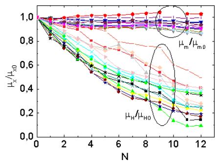
The main task for this experiment was to investigate how quantity and orientation of large-scale structural defects influence measurements of Hall and magnetoresistance (MR) mobilities.
With reference to earlier done experiments [1-4], an attempt was made to experimentally model similar characteristics of samples and to measure them. Large-scale defects can form naturally during growth process or made artificially. It is possible to face distortions of measured parameters when trying to evaluate charge carry parameter – mobility. In this experiment lead telluride (PbTe) was chosen due to its high mobility value. Thin layers were etched in certain patterns which distorted potencial profile. Therefore, measured characteristics (resistance, Hall voltage) were affected. Samples were made using thermal vacuum evaporation method. Ohmic contacts were made out of lead and bismuth mix. AV characteristics were measured to check whether ohmic contacts were good. During experiment, PbTe samples were placed in cryostat and Hall and MR measurements were taken. After that a single defect was etched in the sample by needle under a microscope and measurements were repeated again. Experiment was repeated several times to have more statistical data.
Figure 1 shows substantial difference visible between Hall and MR signals. Large-scale defects influence Hall signals much more than MR signals. It could be explained that to make Hall voltage signal electrons are needed to concentrate in their respective contacts. Defects create obstacles, thus fewer electrons reach contacts. However, to create MR signal, a few electrons are needed because relative change of resistance in magnetic field is being registered.