Silicon remains as the main material used in microelectronic and solar cell industry, because of its low cost, abundance in nature and well-established technologies. To control material wettability [1] and [2], optical properties [3], or field emission efficiency, structuring of the silicon surface was performed. One of the technique used for surface structuring is direct laser ablation. Most of the studies on such Si structuring deal with the formation of self-organized surface structures like sub-wavelength laser-induced periodic structures [4] created by irradiating silicon with multiple femtosecond laser pulses of near-IR radiation.
In this paper, we present the results on patterning of crystalline silicon surface using Direct Laser Beam Interference Patterning (DLIP) technique. This technique uses the interference of several beams to directly pattern the material surface [5]. This technology allows structuring big surface area using only one laser impulse. Ablation with interfering beam was implemented using interference of four and six beams. The laser beam was split into four and six beams by the diffractive optical element (DOE), then those beams were directed on the sample surface using two lenses arranged in 4F system.
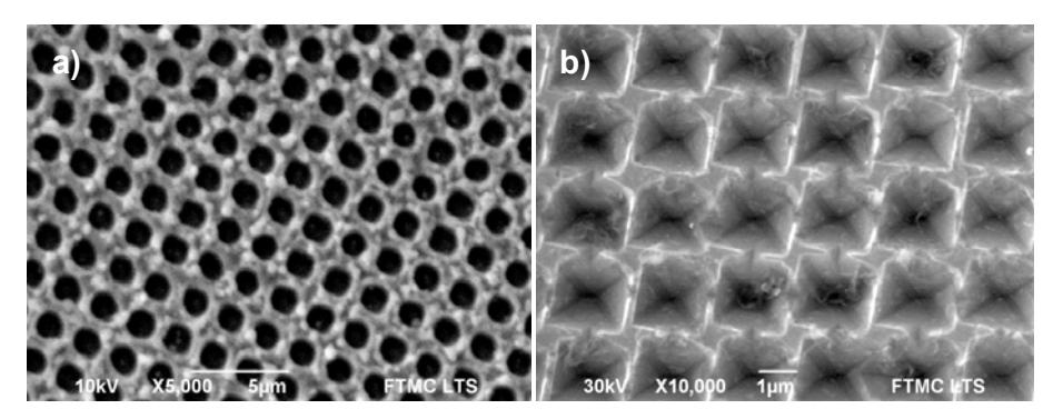
"EKSPLA" 532 nm picosecond laser with a maximum pulse energy of 1.5 mJ and 2-axes positioning system "Aerotech" were used. 1 cm2 silicon plates were ablated using different number of pulses with various energies and after that silicon plates were etched with KOH solution. After etching the plates were examined using SEM, AFM and optical microscope. Results show that after etching, silicon surface forms periodical inverted pyramids (Fig. 1).