Molybdenum ditelluride (MoTe2) belongs to a large group of layered transition metal dichalcogenides (LTMDs). Such materials exhibit unique physical properties that results from the transitaion from bulk to two-dimensional materials, which makes them interesting research subjects. Like other LTMDs, MoTe2 is an inorganic compoundwith hexagonal crystalline structure, with a weak interlayer van der Waals bonding and strong intralayer ionic-covalent bonding. A single layer of this material consists of one plane of molybdenum atoms sandwiched between two planes of telluride atoms with trigonal prismatic coordination, and is a direct-gap semiconductor with a band gap of around 1.1 eV, while bulk material is a semiconductor with an indirect band gap of about 1.0 eV [1].
In this communication, we report our research on the optical properties of MoTe2 crystals, thinned down by exfoliation with a high-quality backgrinding tape and transferred onto a Si/SiO2 substrate with the aid of an all-dry, non-deterministic, polydimethylsiloxan-based stamping technique [2]. We found such an approach to be especially well suited for cleaving LTMDs, which as compared to graphite are much more brittle, and thus turning them into a form of thin flakes with an area that is sufficient to be probed with a laser beam, represents a challenging task. The optical properties of our sample were studied by micro-Raman spectroscopy
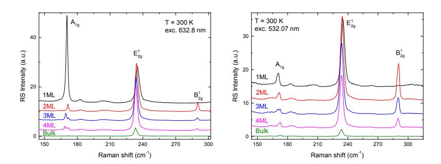
The Raman scattering measurements have been carried out in two excitation modes using wavelengths of $\lambda = 632.8$ nm and $\lambda = 532.07$ nm as a function of layer number of MoTe2 (Fig. 1). Due to the first-order Raman scattering processes a few peaks, including the in-plane E2gl mode ($\sim 234$ cm-1) and the out-of-plane A1g mode ($\sim 170$ cm-1) for monolayer and few layer MoTe2 can be seen. It can be noted that both E2gl and A1g modes are sensitive to the MoTe2 layer thickness, which can be used to unambiguously identify single-layer material. An inactive mode B2gl ($\sim 289$ cm-1) in bulk can be noted for bi-, tri- and four-layer MoTe2 which may be due to the breaking of translation symmetry [1] and has the highst intensity for two-layer material, then we can observe the intensity to decrease with the increasing number of layers of MoTe2.
This study may lead towards further understanding the lattice dynamics and optical processes in LTMD materials, such as MoTe2.