
A variety of the wide band-gap semiconductors, for example GaN, are promising materials in design and fabrication of radiation tolerant particle detectors. The applicability of these materials is grounded on their low leakage currents, effective pair production of secondary charge carriers and radiation hardness [1-2]. Crystalline GaN layers show additionally the rather efficient luminescence properties under the impact of the high energy particle beams. Moreover, it can be also employed not only as scintillating, but also as a charge collecting device [3]. Although efficient GaN p-n junctions are still a pursued objective, the capacitor-type detectors made of the homo-epitaxial GaN layers can already be implemented.
In this work, the tentative capacitor- type device has been manufactured using a 25 μm thick GaN nitride epi-layers grown by MOCVD method on a sapphire substrate (Fig. 1 a). In order to make a capacitor-type device structure, the as-grown layer was plasma etched in three sub-sequential steps using a mask to expose a local sample area to plasma etching. Electrodes were formed by metallization on these etched (three separate) contact spots (marked '1', '2' and '3'). Barrier evaluation by linearly increasing voltage (BELIV) technique [4] and C-V characterization have been employed in order to evaluate the electrical characteristics of the structure and the influence of the contacts to the overall performance of the device. The role of the additional background illumination has been investigated using a UV source.
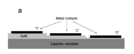
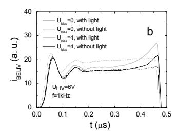
Fig. 1b illustrates the typical responses of the capacitor charging currents under the linearly increasing voltage pulse. As can be deduced from figure 1b, the character of the BELIV transient is dependent on the applied pulsed and dc voltages ($U_{LIIV}$, $U_{bias}$) and on the additional cw illumination. The square-wave shape BELIV transient $i_{BELIV}$, inherent for the capacitor-type device under a single LIV pulse with rearward generation current component, is observed. The initial square-wave component of the BELIV transient is specific for the GaN capacitor. The background UV illumination leads to the increase of both current components within transient, determined by increase of the capacitance of the structure due to the injected charge and that caused by thermal emission via de-trapping from deep levels. This effect proves the possibility to detect the injected charge and temporal variations due to carrier drift and trapping, and functionality of the capacitor-type sensor. The impact of thermal emission current can be modified by de voltage pedestal combined with a pulsed LIV voltage. Thereby, operational characteristics of the sensor and its sensitivity relative to carrier drift signal can be externally manipulated. In summary, the functionality of the capacitor-type sensor made of the MOCVD GaN has been demonstrated. The results of the comparative study of the GaN detector capacitance-voltage (pulsed and dc) and the capacitance-frequency (for harmonic test signals) characteristics will be presented and discussed.