The application of terahertz (THz) radiation in security and medical diagnostics besides sensitive THz detectors also requires developing compact high-power THz emitters performing at room environment. High up to 1.8 μW power emission with power conversion efficiency of 1.6×10⁻⁶ in the range of 0.5-4.0 THz have been observed from AlGaN/GaN field effect transistors (FETs) with sub-micron grating Ohmic contacts at room temperature [1]. The approach was left without obvious explanation and many groups worked on THz emission of the AlGaN/GaN based transistors with Schottky gate grating. In this work we perform comparative analysis of the spectra of THz emission of the AlGaN/GaN FETs with Ohmic and Schottky grating electrodes.
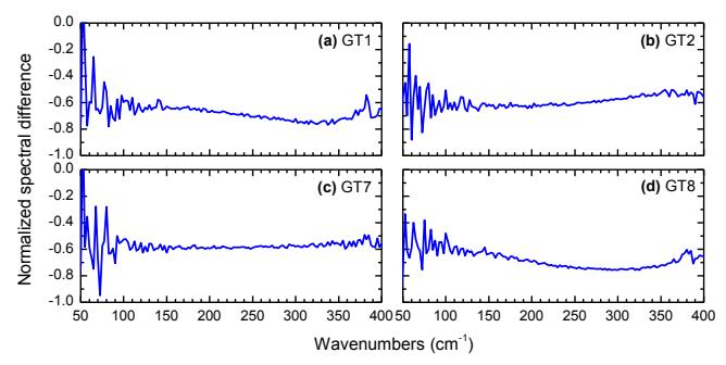
The electronic devices on AlGaN/GaN/sapphire grown in the VU TMI MOCVD reactor were fabricated using recently developed procedures [2]. The carrier density and mobility of two dimensional electron gas (2DEG) in high electron mobility transistor (HEMT) structures was of about 4.7.1012 cm-2 and 2550 cm2/(V·s), respectively. Plasmons excited in FET channel cause electromagnetic waves radiation via the 2x2 mm2 grating of the period ranging from 6 to 150 μm fabricated as the source/drain (Ohmic type grating) and gate (Schottky type grating) contacts. The spectrum of thermally stimulated emission of the samples was measured with Fourier transform spectrometer with vacuum option, and the absolute power - with THz power meter (Thomas Keating). To see the influence of plasmonic grating, measured emission spectrum was normalized
$$(I_{\text{HEMT}} - I_{\text{surface}}/I_{\text{surface}}), \tag{1}$$here $I_{\text{HEMT}}$ is thermal emission spectrum from the FET with grating electrodes, and $I_{\text{surface}}$ – emission spectrum of the AlGaN/GaN/sapphire without any metal electrodes. In such a way normalized spectra are shown in Fig. 1.
The frequency of 2DEG plasma waves in transistor channel was described as [3]:
$$f = \frac{sn}{4L} \left( 1 - \frac{v^2}{s^2} \right), \quad s = \sqrt{\frac{eU_0}{m}}, \tag{2}$$here s is plasma wave velocity, v – average electron drift velocity, L – length of transistor's channel, n – number of plasma wave mode, e – the electron charge, U0 – applied voltage to the FET channel, m – the electron effective mass. For AlGaN/GaN 2DEG, s is around 2×108 cm/s and L was set by the grating period. The first 2DEG plasmon resonance was at lower frequency range 0.25-0.33 THz (9-12 cm-1) for used 6-8 μm period gratins. But indistinct higher plasmon modes in radiation spectrum of the FET with 6 and 7 μm grating period only were observed at 65-100 cm-1 for both Ohmic and Schottky gratings (GT1, GT2, and GT8 samples). Measurement of an absolute power emission from FET with 8 μm period Schottky type grating indicated that the electrical-to-optical conversion efficiency was of about 10-3 in frequency range of 0-10 THz.