Realization of planar integrated optical element with sub-wavelength feature requires advanced lithography techniques, e.g. UV contact, electron beam, nano-imprint lithography, etc. These tools are expensive and bulky. Using one UV laser light source distributed between two optical setups, i.e. Direct Laser Writing (DLW) and Lloyd's mirror interferometer systems, we were able to pattern micrometer range features together with 150 nm sized lines [1].
In a current Lloyd's mirror holographic lithography setup a continuous wave solid state UV laser (371 nm wavelength, 15 mW power) beam is expanded with micro objective and filtered with a spatial filter. Half of the laser beam illuminates the sample directly while the second half is reflected from the mirror and interferes with direct beam on the sample surface. Adjusting the angle of incidence one can control the pitch of the interference fringes. Motorized rotational stages provide precise angle control, i.e. pitch of the fringes can be varied from 300 to 500 nm. Interference fringes were recorded on flat substrates spin coated with negative tone photoresist.
Using DLW setup we have fabricated test structures with few micrometer resolution. The diameter of laser beam spot focused on the sample surface was reduced down to 5 μm. Using precise XY stages and translation of the negative tone photoresist coated sample we have exposed various tests. Exposition doses and steps between adjacent expositions were optimized to obtain micrometric resolution structures.
Automated exposure, selection of the pitch and sample translation for DLW are controlled from one software. After exposure with both optical systems light affected areas in the photoresist film are cross-linked and become insoluble after developing in appropriate solution. Microstructures were analysed employing scanning electron (SEM) and optical microscopes.
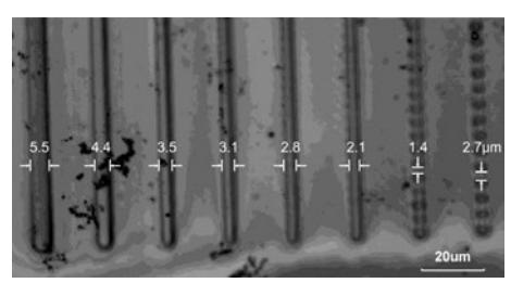
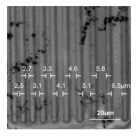
Employing described optical setup test structures including texts, simple integrated optics elements and more complex planar structures were realized. System capabilities changing the point density were demonstrated and smooth lines were obtained employing 1.825 μm step between adjacent points (see Fig. 1). Then lines with different interline distances were exposed employing optimal point density. It was demonstrated that 2.5 μm gap between 3.5 μm spaced lines can be realized (see Fig. 2).