
Metalorganic chemical vapor deposition (MOCVD) is recognized as the method of choice for the large-scale production of nitride based optoelectonic and electronic devices [1]. The group-III-nitride semiconductors (AIN, GaN and InN) and their alloys are promising materials for many optoelectronic device applications such as blue-green and UV light-emitting diodes (LEDs), laser diodes (LDs) and high-temperature, high power electronic devices. The growth conditions affect the Al incorporation and quality of AlGaN epilayer. For these devices, one important thing is to obtain high-quality AlGaN epilayer with high Al content [2].
The main goal of this work was to obtain high crystalline quality AlGaN epilayers with different Al concentration. AIN and AlGaN epilayers were grown on c-plane sapphire substrate by MOCVD (AIXTRON 3x2 FT) reactor. Trimethylgallium (TMGa), Trimethylaluminum (TMAl) and ammonia (NH3) have been used as precursors for gallium, aluminum and nitrogen respectively. All AlGaN samples were grown on 280 nm AlN buffer layer deposited at 1135 °C under hydrogen (H2) atmosphere. The summary of AlGaN growth parameters is shown in Table 1.
| Sample | Template | P, mBar | T, °C | NH3, mol/min | TMG, mol/min | TMA, mol/min | Growth time, s | Thickness, nm |
|---|---|---|---|---|---|---|---|---|
| 452 | 100 | 9,5×10⁻⁶ | 2,9×10⁻⁵ | 4500 | 280 | |||
| 460 | 100 | 2,9×10⁻⁵ | 2,9×10⁻⁵ | 3300 | 420 | |||
| 461 | Sapphire/AlN | 100 | 1090 | 1,8×10⁻¹ | 6,6×10⁻⁵ | 2,9×10⁻⁵ | 4500 | 1120 |
| 463 | 100 | 1,6×10⁻⁴ | 1,7×10⁻⁴ | 3300 | 1120 | |||
| 464 | 85 | 6,6×10⁻⁵ | 6,7×10⁻⁵ | 2700 | 700 |
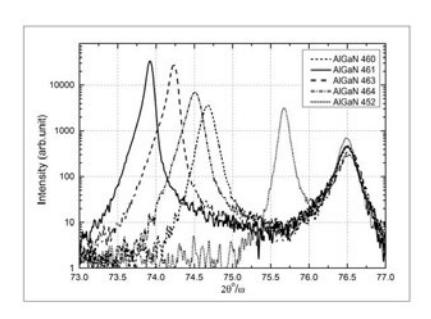
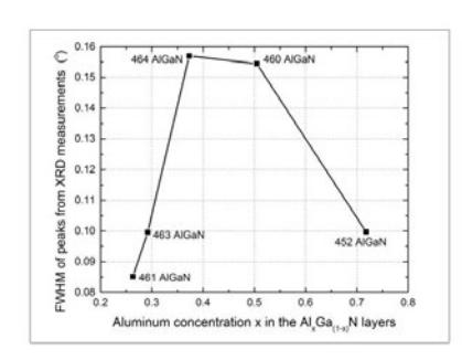
The crystal quality of AlGaN layers and Al concentration has been evaluated using high resolution X-ray diffraction measurements (HRXRD) (Fig. 1). The obtained value of aluminum composition in the layers varied from 26% up to 72%. The value of the full width at half maximum (FWHM) of XRD peaks shows the distribution uniformity of aluminum and gallium in the layer. The dependence of FWHM versus Al concentration revealed that the metal distribution in AlGaN alloys becomes most uneven when Al and Ga concentrations in the layer are similar (Fig. 2).
The surface morphology and roughness of AIN and AlGaN have been studied by atomic force microscopy. Root mean square roughness values have been found to increase from 0.9 nm up to 30 nm with the increase of Al concentration in the AlGaN alloys.
The optical properties of AlGaN/AlN layers have been investigated by room temperature photoluminescence. It was found that with increasing Al content, the AlGaN photoluminescence emission peak shifts towards higher photon energies. A bowing parameter b of -0.61eV was obtained from the band gap variations as a function of Al composition.