
Over the last years, terahertz (THz) radiation from semiconductor surfaces illuminated by femtosecond laser pulses is finding multiple applications areas. It has recently been reported that nanowire and nanorod structures in comparison with bulk semiconductors are able to enhance THz emission from optically excited surfaces. THz emission from low temperature grown InN nanorods was about one order of magnitude greater in power than that from the bulk InN film [1]. Seletskiy et al. [2] reported that their InAs nanowires (NW) had about 15 times greater THz power efficiency than a planar InAs substrate, but this result was obtained after accounting for spatial fill factor in NW arrays. Despite the increase of the efficiency of optical-terahertz radiation conversion vertically aligned nanowire arrays have the same limitation (i. e. the main part of the radiation propagates in parallel to the surface resulting the low THz emissivity outside the sample) as bulk semiconductors. In this work THz emission of the oblique nanowires was investigated for the first time.
In the present work, THz pulse emission from samples of GaAs NW grown by molecular beam epitaxy (MBE) on high temperature (550°C) GaAs (111) and (110) substrates has been studied. One NW layer was epoxy encapsulated and removed from substrate. Experiments have been performed using Ti:sapphire oscillator generating 150 fs, 800 nm pulses at the repetition rate of 76 MHz. THz electric field transients were detected with a low temperature grown GaAs antenna.
The amplitude of the THz signal obtained from NW was from 2 to 4 times stronger than from GaAs substrate. THz pulse amplitude was insensitive to the azimuthal angle for the NW grown on (111) orientation substrates. In contrast, the azimuthal dependencies for NW layers grown on (110) substrates can be approximated by $\sin\theta$ function. The dependencies can be explained by orientation of NW regarding to the GaAs substrate: it is known that the angle between the NW and the surface is 55° [3]. Photoexcited carriers moves along the NW and creates linearly polarized THz radiation. The polarization axis moves around a terahertz beam when an azimuthal angle is changing. The registered signal changes in the sinus's law as the detector registers only one polarization (Fig. 1).
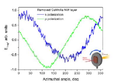
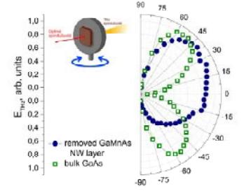
Fig. 2 shows dependencies of THz pulse amplitude on an angle between the incident laser beam and a normal to the sample for the epoxy encapsulated GaMnAs NW layer and GaAs substrate. No terahertz radiation is registered when laser beam falls perpendicularly to the surface of GaAs substrate because the radiation cannot propagate along axis of photoexcited electron-hole dipole. In contrast the NW layer emits the THz radiation well enough as the GaMnAs nanowires are not perpendicular to the plane of the layer.
THz emission of the tilted nanowires was investigated for the first time. The investigated layers can be used in polarization rotating terahertz emitters. This application is very important seeing that the principle of half wave plate can not be used with a wide spectrum of THz pulses.