The development of light sources based on III-nitride compound semiconductors has made a great progress in a recent decade. This is because of the wide spectrum of possible applications and a demand for efficient In(Ga,N) light-emitting diodes (LEDs) with a high power output. The latter is limited by non-radiative losses, which grow noticeably at high charge carrier densities (droop effect [1]). To overcome this unwanted phenomenon and to optimize the devices (and preferably to get efficient emission in the green or even red parts of the visible spectrum) different LED structures are designed and explored.
In this work three sets of samples with different LED multilayered structures, emitting light near 450 nm, are investigated. All samples were grown at the Institute of Applied Research, Vilnius University, on sapphire substrates. The first set consists of two samples with different growth times of quantum wells (QWs), the second consists of two samples with and without short period superlattice (SPSL) and the third set consists of three samples with different growth modes of QWs.
The investigation was carried out using photoluminescence (PL) and differential transmission (DT) techniques [2] in order to track spectral changes in the samples. One of peculiarities of this study is that both techniques were carried out simultaneously, at exactly same excitation conditions. The optical parametric amplifier (OPA) allowed a selective excitation of quantum wells in the samples with a 382 nm (3.24 eV), 250 fs laser pulses.
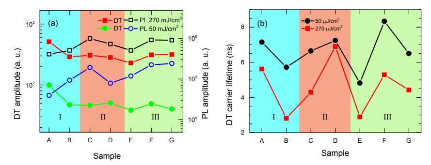
The results of the first set of samples show that twice longer QW growth time (from 58 s to 115 s) gives a clear redshift to both the PL and DT spectra. This can be explained by a weaker quantum confinement as the QWs are wider and by a probable stronger piezoelectric field. The latter might also be responsible for the decrease of PL intensity (Fig. 1a) and possibly for the longer spectrally integrated DT charge carrier lifetime (Fig. 1b), as the electrons and holes become spatially separated. The redshift is likewise seen in the set of samples with the addition of the SPSL, along with higher PL intensity, which proves that the use of SPSL is beneficial. However, carrier lifetimes drop, and the reasons for such behavior are not completely clear.
Another set of samples exhibits longer charge carrier lifetimes and higher PL outputs with application of pulsed QWs growth instead of a non-pulse mode. These results suggest that a better crystal quality in the QWs is achievable. In addition to this, changing durations of metalorganics (MO) flow (samples F and G, MO flow 15 s on/ 5 s off and 15 s on/ 10 s off accordingly) may also alter carrier lifetimes, which indicates, that further optimizations are possible.