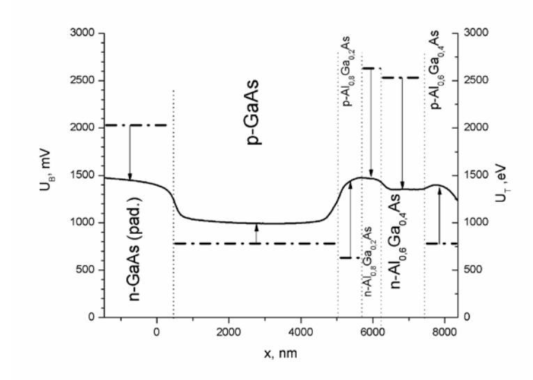
Few last decades electronic components, such transistors, diodes and even components of solar cells, are being scaled down to nanometer dimensions, due to the cost of materials and possible use of new previously unknown physical phenomena such memory resistance or memristance [1]. These actions require a subtle technique in order to measure electrical parameters of these elements with the least possible effect on the component. A growing use of scanning probe microscopy (SPM) based techniques enables new ways to build and investigate nanoscaled electronic devices [2]. Despite of the wide use of SPM in nanoscale surface characterization, the interpretation of the electrical signal and extraction of common electrical parameters of the device remains challenging. SPM usually measures electrical signal at the sample surface (up to few nanometers) but not the bulk.
In our work we used several SPM electrical characterization modes to measure electrical characteristics of the freshly cleaved multilayer AlxGa1-xAs photovoltaic element in room temperature in air. The results were compared with a simple theoretical model. This comparison showed a mismatch between the experimental values and the theoretical ones (Fig. 1). The mismatch was explained in terms of the surface effects, which cause energy band bending at the surface.