
Diluted (GaIn)(AsBi) layers compared to other III-V compounds have weaker bandgap energy temperature dependence, which would be advantageous for the applications in optoelectronics. Alloying GaAs with InAs shifts down the conduction band edge, whereas Bi incorporation has a strongest effect on the valence band states moving up due to the band anti-crossing effect. By a proper selection of the In and Bi content, it is possible to realize the situation at which both conduction and valence bands will move towards each other symmetrically.
The aim of this work was to growth quaternary (GaIn)(AsBi) layers on semi-insulating (100) GaAs substrates in the molecular-beam-epitaxy (MBE) reactor and characterize them.
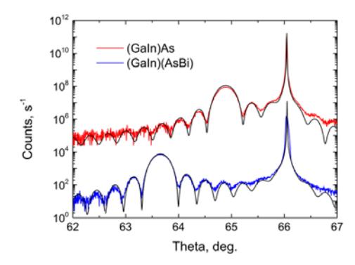
Initially, a test 30 nm thick strained (GaIn)As layers were grown at 240 °C with In concentrations range from 11% to 18% this temperature. Quaternary (GaIn)(AsBi) layers of the same thickness were grown afterwards by keeping group III elements flux unchanged. Its composition was found from the fit of X-ray diffraction (XRD) rocking curve keeping that Ga to In ratio in this layer was the same as in previously grown ternary alloy without Bi (Fig. 1).
Thick (GaIn)(AsBi) layers (~1.1 μm) were grown on the same conditions as the thin layers varying In concentration from 8% to 20% and Bi concentration from 3% to 12%. Thick layers were analyzed using Energy-Dispersive X-ray spectroscopy (EDX), XRD Reciprocal Space Mapping (RSM) and atomic force microscopy (AFM). AFM evaluation showed that samples were rather smooth. For 30 nm thick layers their Root Mean Square (RMS) values were less than 1 nm, for thick layers RMS was several time larger. However, when Bi/As ratio is not optimal metallic Bi droplets appears. From EDX measurement In/Bi ratio in thick quaternary layers was determined. In RSM the maximum corresponding to the layer stays near the line corresponding to a fully relaxed material what mean that only a small residual strain is present in the material. RSM also allows evaluating composition of the layer. Band gap values calculated from EDX and RSM results correlates with band gap values measured from induced THz absorption measurements. This good correlation of data obtained by employing very different experimental techniques provides an additional evidence of their reliability.
Good quality quaternary (GaIn)(AsBi) layers were grown by MBE on GaAs substrates. The layer composition was determined by XRD and EDX measurements and has evidenced an unexpectedly large, of the order of 10%, Bi incorporation resulting in narrower than 0.7 eV energy bandgaps of the material. The structural quality of the layers was even better than that of Ga(AsBi) grown on GaAs substrates with the same Bi content.