Zinc oxide is a multifunctional material with possible application in optoelectronic, ZnO has wide direct band gap of 3.37eV and large exciton binding energy of 60 meV at room temperature. Due to the hexagonal structural symmetry, ZnO exhibit a strong lattice polarization field along the polar c-axis. This polarization field, called Quantum Confined Stark Effect [1], significantly degrades the internal quantum efficiency of the emitting devices. Several groups have used different approaches to solve this problem. A useful approach is to grow ZnO along different crystallographic directions.
We investigated the optical properties of polar c-plane and non-polar a- and m-plane ZnO epitaxial films grown on LiGaO2 (LGO) substrate. The ZnO films were grown by chemical vapor deposition (CVD) directly on the LGO substrate without any buffer layer. Optical characteristics of polar and non-polar ZnO thin films were investigated employing transmission, temperature-dependent photoluminescence (PL) and spectroscopic ellipsometry (SE) techniques. Transmission spectroscopy was carried out using UV-3600 Shimadzu Spectrophotometer, for the PL investigations sample was excited by a diode-pumped Nd: YAG solid state laser working at 266 nm wavelength. Transmission and PL measurements are not sensitive to sample optical anisotropy, to reveal polarization dependent properties we used generalized spectroscopic ellipsometry technique. SE measurements were carried out by dual rotating compensator ellipsometer RC2 (J. A. Woollam Co, Inc.) in the 0.73 – 6 eV spectral range, at the incident angles from 45 to 75 degrees.
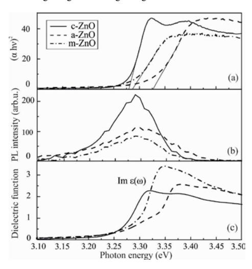
Experimental absorption spectra, presented in Fig. 1 (a), allowed us to reveal fundamental absorption edge, which was 3.276 eV for c-ZnO, 3.325 eV and 3.280 eV for a- and m- samples. Room temperature PL spectra, presented in Fig. 1 (b), show exciton emission maximum at 3.284 eV for c- sample and 3.296 for a- and m- samples. Small exciton emission peak blue shift of about 12 meV related to different exciton binding energy and different band gap values [2]. Spectroscopic ellipsometry allowed for reliable determination of film thickness: a-ZnO and m-ZnO were 124 nm and 408 nm thick and sample c-ZnO - 167 nm. Experimental SE data were analyzed in terms of three phase model, where ZnO dielectric function was characterized as B-spline function [3]. Deduced imaginary part of the ordinary dielectric function presented in Fig. 1 (c). As seen from a figure, all three samples exhibit optical feature at 3.378 eV, which is related to optical transition at $\Gamma$ point. Optical feature at 3.316 eV energy is related to exciton absorption and correspond exciton binding energy of 62 meV. Sample a- and m- show more suppressed exciton absorption than c- one. Determined values of optical band gap and exciton binding energies are in a good agreement with literature data [2].