
Gallium nitride (GaN) is one of the most promising semiconductor materials for high frequency and high power electronics applications, where silicon faces fundamental challenges. High electron mobility, high saturation velocity and breakdown voltages, also very high thermal and mechanical stability are main parameters that encouraged fast GaN-based devices development during recent years [1]. Formation of GaN/AlGaN heterojunction allows two dimensional electron gas (2DEG) to appear at the interface without an intentional materials doping. High carrier mobility and density of the 2DEG are suitable for development of the field effect transistors (FETs) used in radiofrequency power electronics [1]. Moreover, parameters of 2DEG in GaN/AlGaN make possible recent progress of plasmonic THz emitters for efficient operation at room temperature [2]. All of the mentioned applications require good performance of Ohmic and Schottky contacts.
The aim of this work was the investigation of GaN/AlGaN/sapphire structures grown with and without internal super-lattice in Vilnius University Institute of Applied Research (VU TMI) MOCVD reactor. Specific ohmic contact resistance, 2DEG layer sheet resistance and Schottky barrier diode parameters were investigated. Fabricated Ohmic Ti/Al/Ni/Au and Schottky Ni/Au contact structures are shown in Fig1. The structures were fabricated in Semiconductor Physics Institute of Center for Physical Sciences and Technology employing recently developed procedures [3].
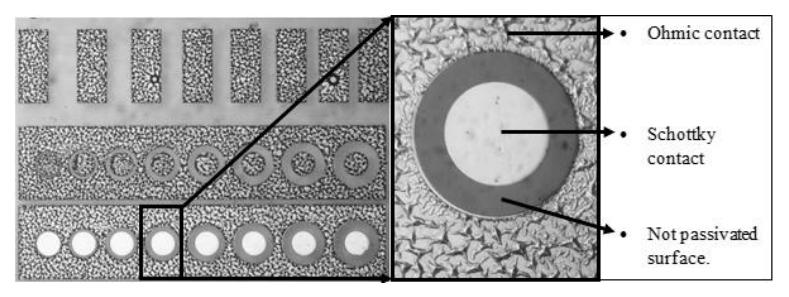
Resistance and IV measurements were carried out in room temperature, using probe station and Keithley 2400 source meter. CV measurements were carried out using Agilent 2494A Precision Impedance Analyser. Schottky barrier diode IV characteristics were measured in the range of -2 to +2V in DC regime.
Measurements using Circular Transmission Line Method (CTLM) revealed the specific Ohmic contact resistance of about $10^{-5}\Omega cm$. Such value was acceptable for investigation of parameters of the Schottky diodes. The sheet resistance of 2DEG was $674\Omega/\Box$ in the investigated sample without superlattice and $616\Omega/\Box$ in the sample with the superlattice design. Obtained carrier mobility was also slightly smaller in the superlattice design sample.
Schottky barrier diode IV characteristics revealed that the formation of the superlattice degrades the leakage currents as it increases the concentration of lattice defects and acts as a second conductivity channel. Existence of the second conductivity channel was also proved by the measured CV characteristic of the Schottky diode. The barrier heights $(1 \div 1,1eV)$ and the ideality factors $(1,2 \div 1,4)$ were found from the IV experiments, performed at room temperature, and correlation between these two parameters, indicating parasitic tunnelling channel, was obtained.
All in all it was concluded, that the introduction of the superlattice in the GaN/AlGaN structures creates a second conductivity channel and an increase of the defect concentration. It is harmful in respect of the production of electronic devices therefore the growth of the superlattice requires further optimisation process.