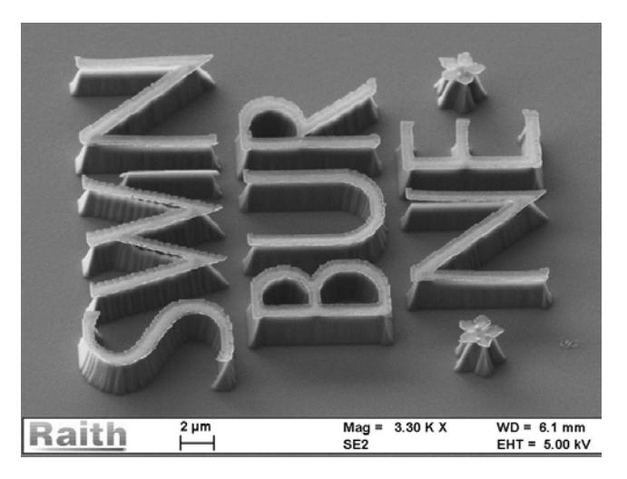
A direct writing lithography technique, via Ga+ ion implantation into the surface of silicon sample, is proposed. Ion implantation is carried out using focused ion beam (FIB) irradiation and subsequent etching is done by an inductively coupled plasma reactive ion etching (ICP-RIE) (SF6 and O2 based plasma). While FIB offers patterning capabilities with sub-micron resolution and ICP-RIE produces highly anisotropic etching profile with high selectivity between ion irradiated and non-irradiated silicon [1], planar (2D) microstructures can be fabricated. The linear selectivity versus implanted Ga density and FIB grayscale micromachining ability enables creation of spatial (3D) structures, which will be shown during presentation.This resistless lithography approach is shown to be suitable for micro electro mechanical systems (MEMS) fabrication.Finally, the removal of masking layer with implanted gallium ions is presented, as well.