
One of the main problems in our world is increasing energy demand and exhaustion of non- renewable resources. The key solution is usage of renewable energy source like solar cell. However, solar cells have relatively high price comparing with other energy resources. To drive silicon solar cells for the further competition in the solar cell market the efficiency must be increased and the price decreased. There is a possibility to increase efficiency and lower the price by using 3D solar cell concept [1]. Another approach to reduce solar cell price is to replace front silver contact (silver price increases so the cell price increases) with other front contact like Ni/Cu [2]. In this work, we analyze the electroplated Ni contact on electrochemically etched porous silicon (por-Si) as 3D solar cell matrix.
As it is shown in fig. 1 main problem in forming contact on por-Si by vapor sputtering is that metal atoms do not fill porous structure inside pores. The advantage of electrolysis is that firstly liquid fills pores with metal ions and then during electrolysis metal can easily cover pores form inside.
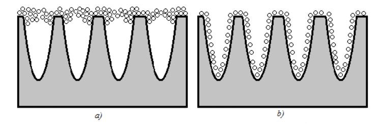
Firstly, the dependence of NiSi formation on annealing temperature was analyzed. Thin nickel layer was by magnetron sputtering deposited on p type silicon wafers. NiSi was formed firing wafers in RTA furnace at different temperatures. I-V characteristics of the samples showed that the ohmic contact was formed for samples annealed at 700°C.
Nickel based electrochemical contact formation was investigated on p type silicon wafers and por-Si samples. I-V characteristics after depositions showed that all formed contacts were schottky type. Samples were annealed at different temperatures and I-V characteristics were measured again. After annealing nickel layer became adhesive to silicon and contact type of all samples changed to ohmic. After measurement of resistivity, it seems that lowest resistivity is for samples annealed at temperatures between 500 – 600°C. It was noted that ohmic with lowest resistivity contacts are formed at lower annealing temperatures than for contacts formed by magnetron sputtering. This is due the silicon oxide removal from the sample surface during electrochemical Ni deposition.