
Black silicon (b-Si) can be described as a semiconductor material which surface is covered with huge amount of densely stacked silicon nano-needles. Black silicon has high absorption of visible light and respectively very low reflectance [1]. This material has wide application – from bacteriological researches [2] to optoelectronic industry [3].
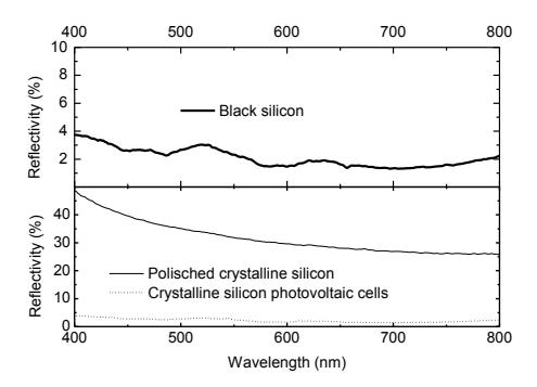
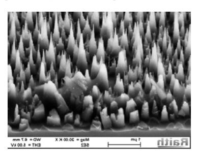
The aim of this research was to optimize technological parameters of reactive ion etching (RIE) process for black silicon fabrication. Optimization was executed in several stages. At first, series of samples were manufactured using dry etching process by adjusting lower electrode's temperature and flow of heat transferring helium gasses in to the etching chamber. Secondly, measurements of an optical reflection spectrum where made for each of the samples (for example Fig. 1), to reveal how optical properties is being influenced by alternating process parameters. Finally, samples were characterized using electrons scanning microscope (SEM) at Swinburne University of technology in Australia (for example Fig. 2), to assess how sample's optical properties is distinguished by nano-needles length and density. After systemizing results of the research a control sample was etched and optically characterized.
Results of the research will be adduced during the presentation.