
One of challenges in producing InGaN light emitting structures lies in deposition of p-type GaN contact layer on top of InGaN quantum well (QW) structures, as these two steps require different growth temperatures. For example in MOCVD growth, the InGaN QWs are usually deposited at temperatures below 900°C, while p-GaN contact layers are best grown around 1100°C [1]. As a result, high temperature deposition of p-GaN may lead to degradation of InGaN QW due to diffusion of In atoms into the surrounding layers. Therefore, there is an interest in growing p-type GaN at temperatures as low as feasible.
In this presentation, we investigate the impact of growth conditions – growth temperature and the precursor flow rate – on the doping level and charge carrier transport in GaN layers. For contactless estimation of hole density, we employ measurement of ambipolar diffusion coefficient, D, as a function of carrier density by Light-Induced Transient Grating (LITG) technique [2]. The set of samples consisted of MOCVD-grown uGaN buffer layers, deposited at 1120°C on top of double sided polished c-orientation sapphire substrate followed by cGaN grown at 1100°C. The layers under investigation were grown at temperatures of 950, 920 and 890°C and at each temperature a set of samples were grown using different Mg precursor pressures of 600, 500, 400 and 300 sccm.
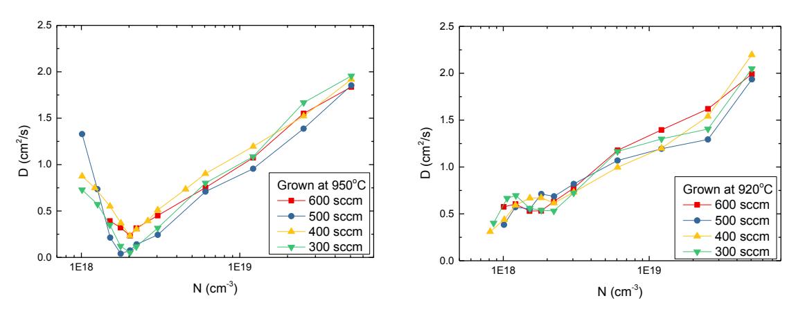
Fig. 1 shows the dependence of ambipolar diffusion coefficient D on photoexcited carrier density N in variously grown GaN layers. The dependence of D(N) in GaN grown at 950 °C has a minimum, while in GaN grown at 920 °C the diffusivity monotonically increases with excitation. We show by modeling that such a behavior of D(N) can be interpreted in terms of ambipolar diffusion in degenerate electron-hole plasma [3]. The decrease of D(N) at lower densities is a signature of p-type doping and can be used for estimation of equilibrium hole density. The results in Fig. 1 suggest that temperature of 920 °C is likely too low for growth of p-type GaN, as the layers are compensated by efficient introduction of n-type impurities. This conclusion is also supported by the dependence of carrier lifetime on growth temperature. The lifetime drops in the samples grown at lower densities, most likely due to higher point defect density in latter samples. In addition, the Mg flow rate seems to affect the mobility of holes as well, which is estimated from D value in the minima of D(N) dependencies.