
The insitu dose control during radiotherapy is important procedure in order to improve the treatment efficiency and avoid detrimental impact on healthy tissues, especially in high dose rate radiotherapy. Therefore, various dosimetry systems, dedicated for dose control during cancer specific treatment, are necessary. These systems require sensors for registering of ionizing radiation. The size of the sensors might also be critical to achieve sufficient spatial resolution. The most commonly used are pMOS (RADFET), direct ion storage (DIS), thermoluminescent (TL) and optically stimulated luminescent (OSL) sensors with specific advantages and drawbacks [1]. Silicon diodes have been used as radiotherapy beam dosimeters, mainly due to their good mechanical stability, high sensitivity per unit volume and high spatial resolution [2]. A new system for the insitu dose control during brachytherapy [3] is being developed at Vilnius University and National Cancer Istitute. However, radiation tolerant sensors of rather small size, high speed and sensitivity are needed for this system.
In this work, the commercial Si sensors of pin structure and active area S=0.35 mm2 have been investigated in order to verify the suitability of the sensors for the brachytherapy system. Sensors were irradiated by 6 MeV electrons, 6 MeV X-rays in the dose range of 0.02 – 6 kGy at National Cancer Institute. Sensors response signals were measured under impact of electron radiation, X-rays and $\gamma$-rays by varying the irradiation flux. Irradiations by electrons and X-rays were performed by TrueBeam/Varian accelerator, while $\gamma$-rays were emitted from 192Ir radionuclide. Current-voltage (I-V) and capacitance-voltage (C-V) characteristics were measured and analysed after irradiations.
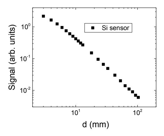
Measurements of I-V characteristics showed that leakage current in sensors increases at highest irradiation doses. This phenomenon can be explained by increased density of radiation defects, which act as generation centres. Analysis of C-V characteristics showed slight variations of effective dopants density in irradiated samples. The sensitivity of sensors was sufficient for registering of signals at distances d$\ge$100 mm between sensor and 192Ir radionuclide emitter of activity $\approx$7.6 Ci (Fig. 1). The largest radiation damage was observed after 6 MeV electrons irradiation.