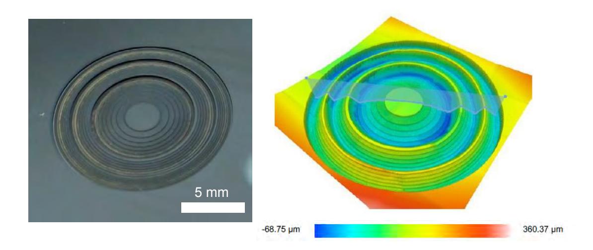
Terahertz (THz) optical imaging is an emerging technology from a wide THz applications research field. From optical communications, spectroscopy to optical imaging through various opaque materials without destruction, it can have possible new concepts and applications as a low-cost platform. Borrowing the conceptual ideas from visible light imaging, the THz imaging can be manipulated and improved by making various diffractive elements that can shape the waves [1]. As the THz radiation wavelength is in the millimeter range, ultrashort pulse laser microfabrication technology can be implemented for the manufacturing of custom diffractive elements on various materials. Using the laser ablation process we can structure the surface of a substrate to control the phase of the incoming THz wave [2].
In this work, we aim for optimized laser ablation process parameters to rapidly manufacture silicon diffractive elements suitable for at least 0.1-0.3 THz range. The aim is to find an applicable processing window that maintains good fabrication quality, avoiding oxidation of silicon and keeping low roughness of the ablated area. Additionally, a comparison of different ablating beam shapes of transformed Gaussian beams using geometric phase optical elements will be conducted to find the best cases for possible microfabrication improvements [3, 4]. In this way, the transformation of the Gaussian beam at the focal zone to a flat-top or C-shaped intensity distribution beam can have a positive impact on the process, such as a reduced heat-affected zone or increased ablation rate.