Vertical-external-cavity surface-emitting lasers (VECSEL) also called optically pumped semiconductor lasers (OPSL) or semiconductor disk laser (SDL) belong to relatively new laser family that combines many of the desirable properties.
VECSELS were developed to overcome key problems typical to conventional semiconductor lasers. In comparison to both types of electrically pumped vertical-cavity surface-emitting lasers (VCSELs), which emit circular fundamental transverse mode beam but exhibit low power and edge emitting lasers (Fabry-Perot and DFB) that can reach high output power but an asymmetric beam with strong angular divergence, VECSELS are capable to generate high optical power with circular beam quality [1].
The output power of such structures is proportional to the area of the emitting surface. Thus, it is very important to grow large area samples of the highest optical uniformity [2]. For this reason, it is necessary to achieve high crystalline quality. In homogeneity, sharpness of interfaces, smooth surface and minimum density of both dislocations and non-radiative recombination centers.
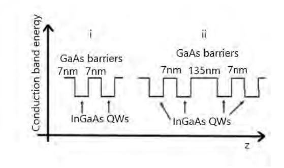
In this work InGaAs/GaAs multiple quantum well structures were grown on semi-insulating GaAs substrate using molecular beam epitaxy technique. MQW structures were targeted to 976 nm operation wavelength. To keep strain balance the investigation and optimization was performed by varying the In content and well thickness. The In content in the QW was varied from 18% to 24.5% and the QW thickness was selected from the range of 3.5-7 nm. Two types of MQWs structures were grown: Fig.1(i) to reach target wavelength simple structures of twelve QW with narrow GaAs barriers of 7 nm were fabricated, Fig.1(ii) for detailed investigation MQW structures containing six double-QW (like in (i) type) separated by wider GaAs barriers of order of hundred nanometers (modelled MQW geometry for VECSEL) were grown. Both types of MQW were studied by HR-XRD to evaluate In content and period of QW and barrier, and to evidence the strain balance. The surface roughness was investigated using AFM. The optical homogeneity of ¼ of 2 inches samples was measured by mapping of PL on a single wavelength corresponding to the maximum of the PL intensity. The effect of different quantum wells design, QW thickness and In content in the well was investigated.